


- 1
- 2
- 3
- 4
CST同轴线器件的仿真设计分析―CST2013设计实例
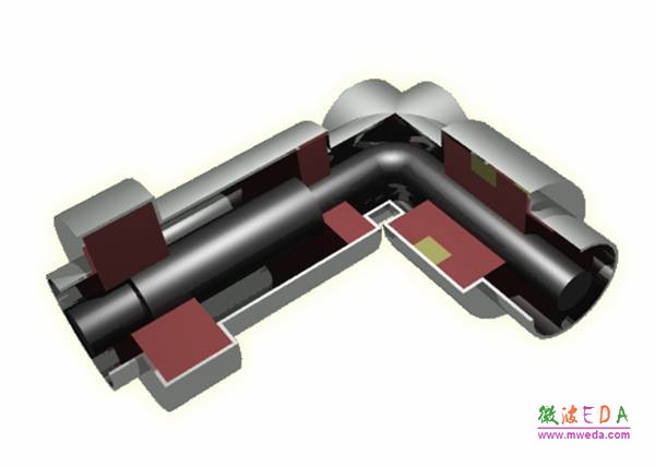
这个设计实例主要介绍和演示如何使用CST微波工作室仿真设计分析同轴线结构器件,设计使用的软件版本是CST2013,所分析的同轴线器件是一个90°的同轴线连接器。
CST微波工作室提供了多种求解器用于分析微波射频器件各项性能,当前设计实例主要介绍仿真分析给出同轴线连接器的S参数. 这里会分别使用时域求解器和频域求解器分析给出同轴线连接器的S参数性能分析结果。
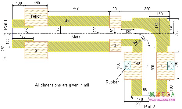
下图是要分析的同轴线连接器结构模型的截面图,图示结构的同轴线连接器包含几段同轴线,同轴线内导体是理想导体(pec),整个结构安放在三个Teflon环上,同轴线内芯和外导体之间的填充介质是真空。
Geometric Construction Steps
This tutorial will take you step-by-step through the construction of your model, and relevant screen shots will be provided so that you can double-check your entries along the way.
Create a New Project
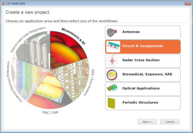
After launching the CST STUDIO SUITE you will enter the start screen showing you a list of recently opened projects and allowing you to specify the application which suits your requirements best. The easiest way to get started is to configure a project template which defines the basic settings that are meaningful for your typical application. Therefore click on the Create Project button in the New Project section.
Next you should choose the application area, which is Microwaves & RF for the example in this tutorial and then select the workflow by double-clicking on the corresponding entry.
For the Coaxial structure,please select Circuits & Components > Coaxial (TEM) Connectors > Time Domain Solver.
At last you are requested to select the units which fit your application best. For the Coaxial structure, please select the dimensions as follows: Dimensions: mil; Frequency: GHz; Time: ns.
For the specific application in this tutorial the other settings can be left unchanged. After clicking the Next button, you can give the project template a name and review a summary of your initial settings:
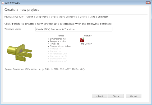
Finally click the Finish button to save the project template and to create a new project with appropriate settings. CST MICROWAVE STUDIO will be launched automatically due to the choice of the application area Microwaves & RF.
Set the Working Planes Properties
The next step is usually to set the working plane properties in order to make the drawing plane large enough for your device. Since the structure has a maximum extent of 1320 mil along a coordinate direction, the working plane size should be set to at least 1500 mil. These settings can be changed in the dialog box that opens after selecting View: Visibility > Working Plane > Working Plane Properties.
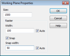
In this dialog box, you should set the Size to 1500 (the unit which has previously been set to mil is displayed in the status bar), the Raster width to 100 and the Snap width to 50 to obtain a reasonably spaced grid. Please confirm these settings by pressing the OK button.
-
CST中文视频教程,资深专家讲解,视频操作演示,从基础讲起,循序渐进,并结合最新工程案例,帮您快速学习掌握CST的设计应用...【详细介绍】
推荐课程

-

7套中文视频教程,2本教材,样样经典
-

国内最权威、经典的ADS培训教程套装
-

最全面的微波射频仿真设计培训合集
-

首套Ansoft Designer中文培训教材
-

矢网,频谱仪,信号源...,样样精通
-

与业界连接紧密的课程,学以致用...
-

业界大牛Les Besser的培训课程...
-

Allegro,PADS,PCB设计,其实很简单..
-

Hyperlynx,SIwave,助你解决SI问题
-

现场讲授,实时交流,工作学习两不误
