Navigation Tree
The Navigation Tree on the
left side of the Main View window
shows and enables the handling of all objects used by CST PCB STUDIO.
Its tree structure provides an overview and supports a detailed investigation
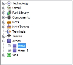
of a PCB. The figure below shows the top level objects:
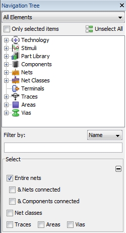
This chapter explains how the objects Nets,
Components, Net
Classes, Traces, Areas and Vias
can be easily browsed and displayed using the Select
function in the Navigation Tree.
For more explanation on items inside the Technology
folder (Layers,
Images and Pad
Stacks) please refer to:
For more explanation on how to generate and edit Traces,
Areas and Vias please refer
to
For more explanation on how to use the extended selection function
provided with the Selection Manager
please refer to
Nets
A Net defines a group of conductive
structures which are galvanically connected. On a PCB there are three
different types of conductive structures: traces,
areas and vias
(see explanation below). Different nets can be assigned to certain net classes. The most important net
classes are signal, power
and ground (see explanation below).
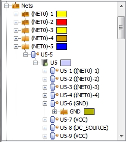
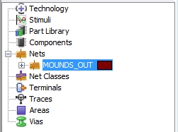
Clicking on the +
sign next to Nets will expand
all nets in the underlying list. Choosing a certain net will highlight
the corresponding structures in the Main
View window. Clicking the +
sign next to a selected will list all pins
that belong to this net. Going further and expanding a certain pin
will show the corresponding component
(device) the pin belongs to. And expanding the component will list all
other pins which can belong to other net instances. This tree-structure
behavior offers a convenient way to explore the inner topology of the
PCB (see figure below):
Selecting a net and clicking the right mouse button will display a
drop-down menu that allows to cut
or copy, to delete
or to edit the net. If Edit is selected from the drop-down
menu a dialog box will be displayed enabling the user to edit five
net parameter as shown below:
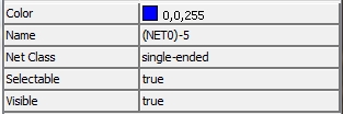
The parameters Color, Name, Selectable
and Visible can be edit via the
Attribute Manager in the View Options window, too (see View
Options Window). The parameter Net
Class can be edited via the Net
Class Manager, too (see Nets
and Net Classes). Selecting the root object Nets
itself and clicking the right mouse button will display a similar drop-down menu enabling the user to
allocate a new net instance.
Components
A component represents a device that can be either placed at the top
or the bottom layer of a PCB. The most important characteristic of a component
is its list of pins. From a geometrical point of view the component's
pins define the place where the connected nets end. This information is
defined and stored in the image
a component refers to (see Components
and Geometric Properties).
From a modeling point of view a component's pin defines the electrical
behavior that can be seen from the connected net. The electric behavior
for each pin can be defined with the help of the Component
Definition dialog box (see Basic
Components Dialogs). Defining the electric behavior of a component
means adding necessary information to enable a complete simulation workflow
within CST PCB STUDIO.
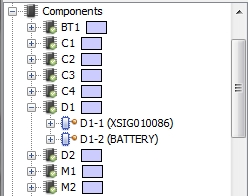
Clicking on the +
sign next to Components will
list all components of the PCB. Choosing a certain component will highlight
the corresponding object in the Main
View window. Selecting a special component in the Navigation
Tree and expanding it will display the corresponding pins of the
component (in the Navigation Tree).
And further, expanding a certain pins will show the corresponding net
the component's pin belongs to (see figure below):
Selecting a component and clicking the right mouse button will display
a drop-down menu that allows the user
to delete or to edit
the component. Selecting the root object Components
itself and clicking the right mouse button will display a similar drop-down menu enabling the user to
call the Component Definition manager
or to allocate a new component instance. For further information on the
editing of components please refer to Basic
Components Dialogs.
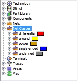
Net Classes
A net class defines a group
of nets that belong together in any certain way. For instance, all nets
providing power can be combined
into the net class power. By
default CST PCB STUDIO provides five default net classes as shown in the figure
below:
Selecting a net class and clicking the right mouse button will display
a drop-down menu that allows to edit
the net class as shown below:
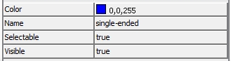
All parameters (Color, Name, Selectable
and Visible) can be edit via
the Attribute Manager in the
View Options window, too (see
View Options Window). Selecting
the root object Net Classes itself
and clicking the right mouse button will display a similar drop-down
menu that allows to allocate a new net class instance or to call
the Net Class Manager (see Nets and Net Classes).
Traces
A net consists of a group of traces,
areas and vias
which are electrically connected to each other. A trace
itself defines a point-to-point section. For further information on the
definition and editing of a trace, please refer to Traces.
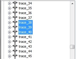
The figure below shows a highlighted net with a branch in its middle:
The structure can be highlighted either by selecting the corresponding
net in the Nets folder or by
selecting the corresponding three traces in the Traces
folder as shown in the figure below:
Areas
Apart from traces, areas are the second geometric structure
type a net can consist of. As with a trace,
an area is always located on
a special metallic layer. For further information on the definition and
editing of an area, please refer to Areas.
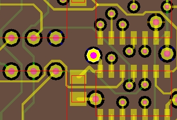
The figure below shows a highlighted area
which covers the whole layer of a PCB:

The corresponding selection in the Areas
folder of the Navigation Tree
is shown in the figure below:
Vias:
A via is the third geometric
structure type a net can consist of. A via
provides the vertical connection between traces
or areas, which are located on
different layers. An important data structure a via
refers to is the pad stack. Pad stacks are defined in the Pad Stacks sub folder, which is located
inside the Technology folder.
For further information on the definition and editing of vias,
please refer to Vias
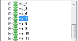
and Pad Stacks. The figure below shows a highlighted via:
The corresponding selection in the Vias
folder of the Navigation Tree
is shown in the figure below:
Filter
The figure below shows a list of many nets which is typical for a PCB:
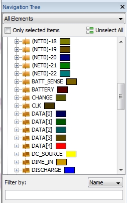
The filter function can be used to reduce the number of visible objects
in the Navigation Tree. The most
general filter function is filtering by "Name". Therefore,
Name has to be selected in the
drop-down menu on the right bottom side (see figure above). In a next
step, the corresponding string parts plus some suitable asterisks (*) have to be
entered in the field below. After pressing the Return
button the view elements will be reduced to the matching elements:
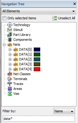
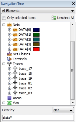
In addition, there are two further filter functions: by "Net"
and by "Net Class". If you repeat the
filtering with the same string ("data*") but with the setting
Net or Net Class(instead of Name),
not only the corresponding nets but also the traces, areas and vias, which are related
to these nets or net classes, will be listed (see figure below):
Selection options
In general, there are two possibilities
to select an object (net, component, trace,
area,via):
The first
option is to select the object directly in the Navigation
Tree (by using the left mouse button). After selecting the object,
it will be highlighted in the Main View
as far as the chosen attributes in the
View Options Window allow any visualization at all (see View
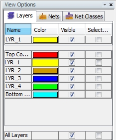
Option Window). To make sure that the selected object can be highlighted,
the user is recommended to switch on All
Layers and All Nets inside
the corresponding tabs of the View Options
Window and to set all listed layers and nets to Visible
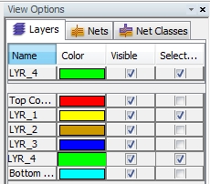
as shown in the figure below:
The second option is to select
the object in the Main View by
double mouse clicking on the
corresponding structure. This will highlight the structure in the Main View but will also select and
mark the corresponding entry in the Navigation
Tree. Because of the layers being on top
of each other, the selection in the Main
View is not always clear. In order to get a better control, the
View Options Window provides
the possibility to decide which layers (or nets) should be selectable
at all. This can be done with the help of the column Selectable
as shown in the figure below (see also View Options Window):
Selecting in the Main View
allows for a quick and convenient exploration of the
PCB. A useful additional function for this purpose is the flag Only
selected items as can be seen in the figure below. If
the flag is activated only objects, which are selected in the Main View,
will be displayed in the Navigation
Tree:
The result of both selection options will be the same either the selection
is chosen via the Navigation Tree
or via the Main View.
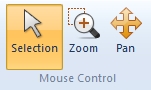
Note:
As a prerequisite to select structures with any
of the two selection options the Selection
view mode for the left mouse button has to be activated by View:
Mouse Control
as shown in the figure below: