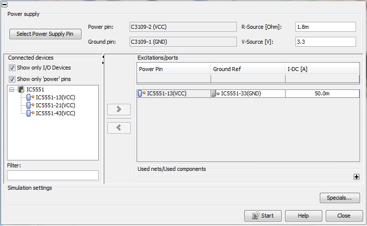
IR-Drop (DC)

Home: SimulationIR-Drop Analysis

The goal of an IR-Drop task is to analyze the amount of voltage drop on a power/ground system by a given DC current consumption on one or more power pins of I/O devices. The power/ground system consists of a power supply device which is connected to a combination of power- and ground nets.  The result of the IR-Drop task is not an equivalent circuit that has to be further processed in a circuit simulation. There are two different result types: First, a set of 0D voltage and current data for the related component pins. Second, a 2D surface current and voltage distribution on the given power/ground conductors. The figure below shows the corresponding dialog box:


The Power supply frame allows the definition of the power supply pin as the central element in an IR-Drop analysis. Once the power supply pin is defined, its corresponding ground reference pin can be automatically determined by the program (see Power Supply Modeling). Furthermore the program considers additional nets which are separated by passive 2-pin components (i.e. resistors) from the directly connected nets using the selection mechanism of the Selection Manager. Finally the program finds the corresponding power pins of the connected I/O devices, which will be displayed in the Connected devices frame (see below).


The Connected devices frame displays the power pins of all devices which are connected to the power- and ground net of the power supply from above. By default, only I/O devices are listed. In order to collapse all pins from all components at once, the user has to right mouse click and pressing Collapse All inside the drop-down menu.


Show only I/O Devices: This button is activated by default.


Show only power pins: This button is activated by default since only power pins can be shifted to the Excitations/ports frame on the side. Switching off the button may be useful to see the overall size and complexity of the device.


Excitations/ports frame

In order to define an IR-Drop task, the user has to select a certain pin inside the Connected devices frame and shift the pin by using the right-direction arrow to the Excitations/ports frame (or by dragging it with the mouse):


Power Pin: Displays the shifted power pin of an I/O device. The field can not be edited.


Ground Ref: Displays the corresponding ground reference pin of an I/O device (see Power Consumption Modeling) . The field can be edited.


I-DC: Displays the DC current consumption of the power/ground  pin pair (see Power Consumption Modeling). The field can be edited.


The Used nets/Used components frame displays all nets which were recognized by the program due to a certain pin selection (see left column). In addition, all passive two-pole components which are connected between the listed nets are displayed in the right column.


Specials settings

Pressing the Specials... button opens a separate dialog box:

The Geometry simplification frame includes three further fields (see also Geometry Simplification for PEEC)


Starting the calculation

Pressing the Start button starts the IR-Drop analysis. This means, in a first step, the program will launch a pure resistive 3DPEEC modelling process (see 3DPEEC). Afterwards, in a second step, a DC task including the complete circuit will be generated in CST DESIGN STUDIO and the circuit simulation will be started. Information on the status of the simulation process will be given in the Message Window. After the circuit simulation has finished the 0D voltage and current data are stored in CST DESIGN STUDIO according to the listed pins inside the Excitations/ports frame. The 2D voltage and current distribution will be stored in a separate Results folder inside the Navigation Tree of CST PCB STUDIO. In a final step, the 2D result viewer (see 2D Result viewer) will be launched in order to display the 2D results immediately.