
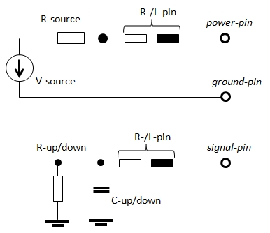
Pin Type: must be power
Ground Ref: enables a 2-pin port, presumes an existing ground pin, see Ground Reference for power supply
Pin Group: optional, see Pin Grouping for power supply
V-source: the voltage of the power supply
R-source: the inner resistance of the power supply
R/L-pins: optional
In order to have a ground reference pin assigned to all signal and all power pins automatically, the user can press the Ground Refs ... button at the top of the table. The corresponding dialog box proposes to assign the ground pin which is closest to a signal (or power) pin as reference.

In order to have a power reference pin assigned to all signal pins automatically, the user can press the Power Refs ... button at the top of the table. The corresponding dialog box proposes to assign the power pin which is closest to a signal pin as reference.
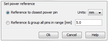
The second option "Reference & group all pins in range" performs to actions in one. It first groups all power pins within a certain range (see section Pin Group below). In a second step the power pin group which is closest to a signal pin will be assigned as reference.