I/O Device Modeling
There are two main modeling aspects on I/O
Devices. The first is to model the behavior of the Input/Output
system, the second to model the behavior of the device's power consumption system. Both aspects
can be treated within one table (see figure below). The aspect that
should be modeled decides on which data fields are to be filled.
Input/Output
Modeling
The central element of
Input/Output Modeling is the signal pin.
Modeling the I/O system
means modeling the current- and voltage relations at the switching
output and the receiving input
pins (both the switching output and the receiving input pin are considered
signal pin). An important characteristic of the signal pin is its inner,
typically non-linear impedance, which has an impact on reflections and
over- and undershoots of the transmitted signal. In
general, every signal pin has to be modeled independently by assigning
an appropriate Signal Model (exception: differential signal model, see below). A Signal
Model includes the inner characteristic impedance
(linear or non-linear) and the transition
behavior during the high-low state
changes (rising and falling wave forms). In addition to the Signal Model,
a Stimulus
has to be assigned providing the corresponding bit sequence for the signal
pin. The I/O Modeling of a certain pin is a prerequisite for its usage
within a SI-TD analysis (see SITD).
The electric current sent out through an output
pin has to be delivered by a certain pair of power-ground pins. In reality,
this has an impact on the voltage between the supplying pair (voltage
ripples, power/ground bounce). CST PCB STUDIO considers the current supply
ideal. An internal feedback from the output pin back to the power/ground
pins is not accounted for.
In order to prepare a certain pin for I/O Modeling the following fields
in the corresponding row of the table has to be filled:
Power
Consumption Modeling
The central element of Power Consumption
Modeling is a pair of power and ground pin (or more general: a pair
of power and ground pin groups,
see below). There are two general reasons for power consumption: First,
power (or current) is needed to supply the I/O signaling. Second, the
internal processes of the device need power, too. The first case can not
be considered as mentioned above (see I/O Modeling).
The second case is considered for DC within the IR-Drop analysis (see
IR-Drop).
In order to prepare a certain pin for Power
Consumption Modeling, the following fields in the corresponding
row of the table has to be filled:
Table
for I/O Device Modeling
The table consists of an upper and a lower part. The upper part consists
of only two rows: the top row
lists the available column types (Pin,
Net, Pin
Type, ...). The row below is the selection
row and includes the data of the currently selected row inside
the lower part. The lower part provides the actual data
table. There are as many rows in the table as device pins. Whether
a certain data field in a row is needed or not depends on the selected
Pin Type.
The rows of the lower data table can be sorted in an alphabetic order
(upwards / downwards) according to any of the available column types.
For example, in order to sort the table data according to net
names, the user has to double click on the Net
field inside the top row!
The table provides a multi-selection
feature: For example in order to assign a certain Signal
Model to two different signal pins, the corresponding rows in the
table can be selected with <shift><left mouse button> (see
figure below). The Pin- and Net names in the selection
row automatically turn to "..."
(means: no unique name is possible). Next, the user has to double click
on the Signal Model field inside
the selection row! A pull-down
menu enables the user to specify a certain Signal
Model which is then assigned to both pins.

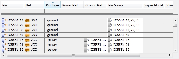
Pin: The column lists all pins
of the corresponding device.
Net: The
column lists the nets the corresponding pins are connected to.
Pin Type
The pin type can not be chosen but depends on the net class of the
connected net. If the pin type should be changed the corresponding net
class of the connected net has to be changed by using the Net_Classes_Manager.
Ground
Ref
A Ground Reference has to
be specified for a power pin and optionally for a signal pin. As a prerequisite
one ground pin has to exist at
least. The combination power pin / ground
reference pin builds a port
to which a DC current can be assigned during an IR-Drop analysis (see
IR-Drop). The combination
power pin / signal pin /ground pin
builds an I/O driver used to switch
current from the power- to the ground conductors via the voltage on the
signal pin (see SITD).
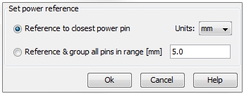
In order to have a ground reference pin assigned to all signal and all
power pins automatically, the user can press the Ground
Refs ... button at the top of the table. The corresponding dialog
box proposes to assign the ground pin
which is closest to a signal (or power)
pin as reference.

The second option "Reference
& group all pins in range" performs to actions in one.
If first groups all ground pins
within a certain range (see section Pin Group below). In a second step
the ground pin group which is
closest to a signal (or power) pin
will be assigned as reference.
Power Ref
A Power Reference can optionally
be specified for a signal pin. The combination power
pin / signal pin /ground pin builds an I/O
driver used to switch current from the power- to the ground conductors
via the voltage on the signal pin (see SITD).
In order to have a power reference pin assigned to all signal pins automatically,
the user can press the Power Refs ...
button at the top of the table. The corresponding dialog box proposes
to assign the power pin which
is closest to a signal pin
as reference.
The second option "Reference &
group all pins in range" performs to actions in one. If first
groups all power pins within a
certain range (see section Pin Group below). In a second step
the power pin group which is closest to a signal pin
will be assigned as reference.
Pin
Group
Pins of type power and ground can be grouped together. From
an electrical modeling point of view this means all pins within a group
will be shorted and will have the same electrical potential. As default,
every Pin Group includes its
own pin, see figure below:

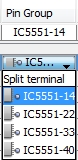
In order to group the ground pins, we start by double clicking on the
corresponding Pin Group field
of pin IC5551-14. A drop down
menu opens providing the two further ground pins IC5551-22
and IC5551-33 as shown in the
figure below:
After selecting IC5551-22
both ground pins are grouped together as indicated by the name IC5551-14,22:

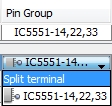
Repeating the procedure by double clicking
on the Pin Group IC5551-14,22
and selecting the remaining ground pin IC5551-33
results in the Pin Group IC5551-14,22,33
as shown in the figure below:
In order
to split pin
IC5551-14 from the Pin Group, double click in its Pin
Group field and select Split
terminal as shown in the figure below:
As a result, pin
IC5551-14 is separated again and builds its own Pin
Group as shown in the figure below:

Note: if
there are more pins to be added to a group the multi
-selection feature mentioned above can be used (see Table_for_IO_Device_Modeling).
Signal
Model
Three different types of signal models are available: Pulse,
IBIS and Differential.
In order to change/edit the existing signal model, double click on the
corresponding Signal Model field
and choose Edit... from the pull-down
menu.
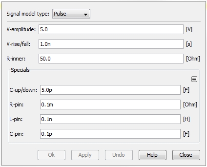
Pulse (default excitation):
Defines a linear voltage ramp in combination with
an inner resistance. In addition, pull-up / pull-down capacitances and
a simple equivalent circuit for the pin parasitics can be specified inside
the Specials frame:
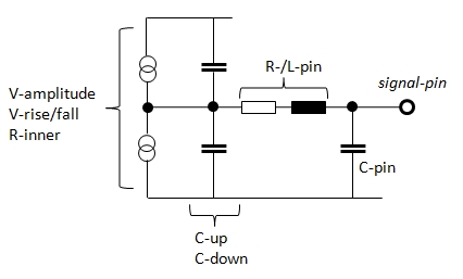
The
internal circuit topology of the Pulse
model is shown in the figure below. The linear voltage ramp and the inner
resistance is made up by a combination of two voltage controlled current
sources.
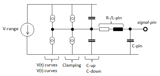
IBIS:
There are two main differences between the standard
Pulse and the IBIS-pin-model:
the first is the possibility to substitute the linear voltage ramp of
the Pulse (consisting of V-amplitude and V-rise/fall)
with a more accurate V(t)-characteristics.
The second is the possibility to substitute the linear inner resistance
(R-inner) with a more accurate
non-linear V(I)-characteristics.
In addition, the IBIS-pin-model can also account for special clamping
characteristics. The internal circuit topology of the IBIS model is similar
to the topology of the Pulse model:
All values and curves
of an IBIS model are stored in a corresponding ASCII file which can be
handled with the following dialog box:
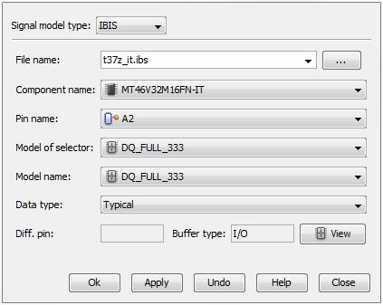
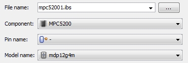
File
name: The field provides a drop-down menu where an imported IBIS-files
can be chosen directly. If a new IBIS file has to be imported the user
has to press the file browser button next to the field on the right hand
side.
Component
name: In general an IBIS file includes the pin description of a
complete device. Further, an IBIS file can include even more than one
single component description. This is mostly the case when different flavours
of a component (i.e. due to different firmware of the
device) exist. The field allows the user to select between different component
models.
Pin
name: In general an IBIS file includes a list of pins. Each pin
has its own type (signal, power, ground)
and (in case of type signal) one
or even more corresponding models. The field allows the user to select
a specific pin.
Model
of selector: If a pin is assigned more than one model the model
selector can be used to assign the right model to the pin.
Model
name: If a pin name has been selected (see above) the corresponding
Model name will be automatically displayed in this field. Furthermore
this field allows the direct assignment of a Model name (from the IBIS-file)
to the component pin without any previous assignment of a Pin name. In
this case the field of Pin name will stay empty as shown in the figure
below:
Data
Type: An IBIS file usually provides three types of models for each
pin model: Typical, Slow
and Fast. Type Slow
represents a U(t) characteristic with the smoothest slopes (long rise-
and fall-times, small amplitude). Type Fast
represents an U(t) characteristic with the steepest
slopes (short rise- and fall-times, high amplitude). The type Typical
represents an U(t) characteristic which is in between.
Diff.
pin: This field is not for editing. It only shows the differential
mate of the pin (defined in the Pin
name field) if such an information is stored in the IBIS file.
Buffer
type: This field is not for editing. Besides the Buffer type I/O (input / output) there are also
pure input types or pure output types available in an IBIS file.
View: Opens the CST IBIS Viewer with the currently
selected pin or model (see CST_IBIS_Viewer).
Differential:
This signal model type enables the user to define
the selected pins as a differential mate of an other pin. The differential
mate owns the same electrical behavior, except the amplitude of the V(t)
curve, which is for one pin exactly the negative variant of the other.
In the corresponding dialog box the only setting is the assignment of
a Differential mate. This can
be done by selecting any of the available pins from the drop-down menu.
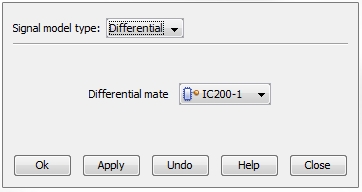
Note: If a differential
mate assignment has been done and one pin has been assigned an IBIS-pin-model
and the other pin a Pulse model:
in this case the IBIS-pin-model will be used for both pins and the previous
model (Pulse or IBIS)
will be removed.
A Stimulus
assigns a certain state sequence to
a standard input/output pin. Three
states are possible:
0: low voltage state of an active output
pin
1: high voltage state of an active output
pin
z: idle state of an passive output pin
By default a signal pin is a standard
input/output pin. But if a signal model is assigned via an IBIS
file it may happen that the pin is converted into a pure
input. For such a pure input
pin no Stimulus can be assigned
as shown in the figure below:

Termination:
This column enables the user to add different kind of artificial termination
networks for every signal pin.
These settings are not mandatory but allow a quick what-if
analysis on the influence of the most common termination networks without
editing the PCB layout first. Six kinds of termination networks are available:
series R: Resistance in series between
the inner signal pin and the
(new) outer signal pin
series C: Capacitance in series between
the inner signal pin and the
(new) outer signal pin
parallel R: Shunt resistance between
the signal pin and ground
parallel C: Shunt capacitance between
the signal pin and ground
RC (parallel): Shunt series R-C- network
between the signal pin and ground
Pu/Pd (pull up/down resistor in parallel):
Two shunt resistances, one between the signal pin and ground, the other
between the signal pin and the power node (= Vrange).
Assign Model...
If an IBIS file does completely match a certain device an automatic
assignment of the IBIS-internal models to the corresponding device pins
can be done. In addition, once the I/O
Device Model settings of a certain component have been exported
in a CST Components Database file (via the Export
Components function, see Export
Components) these settings can be re-assigned to a component with
an identical name.
The corresponding Assign Model... button to enable the
described model assignment is located at the right top of the table:

After pressing the button, a pull-down menu opens where the user can
select between either Assign IBIS Model...
or Assign I/O Device Model....
Assign IBIS Model...

File: Enables
the user to select an IBIS file which has been imported already or to
import a new IBIS file by using the file browser with the button next
to the field on the right hand side.
IBIS models frame:
Lists all component models which are in the selected IBIS-file. The current
model is displayed in the Selected model field.
Assign by pin names:
Only such pins from the IBIS file that match the pin names of the
component are assigned automatically. If no matching was found a message
will be displayed.
Assign by pin indices:
All pins from the IBIS file are automatically assigned to the component's
pins according to their order and with no regard of their names.
Assign I/O Device...
A file browser opens and the user can search for an exported CST Components Database file (see Export
Components).