
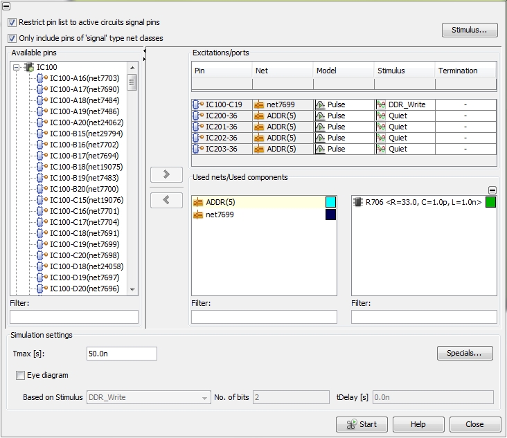

In the figure above just pin IC100-C19 of net net7699 was shifted to the Excitations/ports frame by the user. The other net ADDR(5) was recognized by the program and the corresponding pins of the further components were entered automatically. In order to remove a certain pin (or group of pins), the pin has to be selected and shifted by using the left-direction arrow (or by dragging it with the mouse).
Pin: Displays the pin which was either shifted from the Available pins frame by the user or added automatically by the program. The field can not be edited.
Net: Displays the corresponding net of the corresponding pin. The field can not be edited.
Model: Displays the I/O device model assigned to the pin. Two kinds of active circuit models are available: a simple Pulse model (default) or a more sophisticated equivalent circuit extracted from an assigned IBIS model. Both types of models can be used to define a Differential pair from the corresponding pin and a further pin (see I/O Device Modeling). The field can be edited by simply double-clicking on it with the left mouse button.
Stimulus: references to a pre-defined Stimulus (see Stimulus Editor).
Termination: Allows the user to add a termination network between the pin and the connected net on the PCB from a predefined list (see I/O Device Modeling). This functionality is useful if the user wants to perform a quick what-if analysis without having to change any layout in the first place.

Tmax: specifies the time where the analysis stops
In addition, the user can activate the Eye diagram button which enables an additional output of the simulation results in eye-diagram style. If this button is activated the user has to specify a reference stimulus and the number of bits in order to derive the unique time frame for the eye diagram.
The Meshing Settings frame includes the following four parameters (see also 2DTL Meshing tab):
Search distance for coupling: Parallel segments of different (but selected) nets were considered electromagnetic coupled within this distance (see Search distance for coupling).
Minimum length for coupling: Parallel segments must have a certain minimum length to be accepted for an electromagnetic coupling (see Minimum length for coupling).
Use legacy via model: Defines which kind of via model should be used. For more explanation, see Use legacy via model.
Consider padshapes: Defines whether pad shapes shall be considered or not. For more explanation, see Consider padshapes
Consider meander interaction: Defines whether the electromagnetic coupling between segments belonging to the same net shall be considered or not, see Consider meander interaction
The Model Settings frame includes the following two parameters (see also 2DTL Modeling tab):
Dielectric losses: Specifies whether dielectric losses shall be considered or not (see 2DTL Modeling tab, Dielectric loss modeling).
Model valid up to frequency: Defines the frequency up to which the equivalent circuit must still be valid (see Model valid up to frequency)
The IBIS Settings frame includes the following two parameters (see also Signal Modeling):
Data type: For every IBIS pin model there are three kind of U(t) characteristics possible: Typical (default), Slow and Fast. A pin is always assigned to one of those choices (see Signal Modeling). The parameter allows the user to decide whether the individual choice of the pins should be adapted or all pins should be in general treated either with their typical, slow or fast U(t) characteristics.
Set probes at die: If the parameter is true additional probes are set by the program in order to get voltage/current results for the inner device side of the pins.
The Solver Settings frame includes a single parameter:
Time stepping: Allows the user to control the time stepping algorithm during the transient simulation: fixed auto means the program determines an optimal constant time step, fixed manual time step means the user has to decide for a constant time step and dynamically means the program uses a dynamic time step.