|
微波射频仿真设计 |
|
|
微波射频仿真设计 |
|
| 首页 >> Ansoft Designer >> Ansoft Designer在线帮助文档 |
|
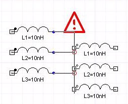
Schematic Editor > Placing ComponentsTo help facilitate the easy copying of design materials, Designer allows you to drag and drop designs, components, and models from the Project Manager window to the Schematic Editor. In particular, you can drag and drop: • A design from the Project Tree to a schematic • A component from the Project Tree Definitions folder to a schematic • A component from the Search tab component list to a schematic • A component from the Components tab component list to a schematic • A model from the Project
Tree Definitions folder to a component in the schematic
To place a component: 1. Select the schematic that will contain the component you place. 2. In the Project Manager window, click the Components tab. 3. In the component list, locate the component you
want to place, opening library files 4. Next, select and place the component in the schematic using one of the methods described in the Note above. You can rotate a component before placing it by repeatedly pressing R on your keyboard. Each press rotates the component 90º counterclockwise. You can flip the component left-to-right by pressing the X key. You can flip the component top-to-bottom by pressing the Y key. For components with physical layers, the Merge Layers dialog box may appear. See the Merge Layers Dialog topic for details. Inside the schematic window, the cursor is accompanied by the component symbol for placement.
NOTES 1. The first time you place a component in a project, entries for it are added under the Component tree’s Most Recently Used and Project Components headings. To save time as your work progresses, you can place new instances of a component by double-clicking these icons as well. Please note that for security reasons, encrypted components are not saved in the Most Recently Used list or the Favorites list. 2. To ensure electrical connectivity among schematic elements, the pins of placed components snap to a 100-mil (2.54-millimeter) grid. This snapping cannot be turned off, and the spacing of the connectivity grid cannot be adjusted. 3. To move an existing component, select and drag
the component to a new position. In-place wiring to the component is
automatically adjusted. To retain the in-place wiring, hold down the
ALT key as you drag the component to a new position.
The topics for this section include: Displaying and Editing Component Properties Favorites and Most Recently Used Components
HFSS视频教程 ADS视频教程 CST视频教程 Ansoft Designer 中文教程 |
|
Copyright © 2006 - 2013 微波EDA网, All Rights Reserved 业务联系:mweda@163.com |
|
 and folders
  as necessary to find it.