|
微波射频仿真设计 |
|
|
微波射频仿真设计 |
|
| 首页 >> Ansoft Designer >> Ansoft Designer在线帮助文档 |
|
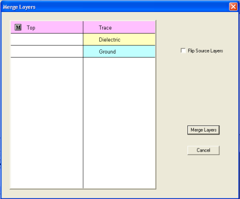
Layout Editor User Guide > Merge Layers DialogWhen a component or object that has a footprint is placed in the layout or in a schematic, Ansoft Designer® must map the layers in the component object to the layers that have been defined for the design. • In a mapping, each layer in the component is either merged with an existing layer in the design or inserted as a new layer in the design. • The mapping is controlled by the Merge Layers dialog. You can specify (with the “Always Show Layer Merging dialog” Layout Editor option; see Layout Editor Options) that the Merge Layers dialog is to be displayed every time a component is placed (the default), or you can have the dialog display only when mapping of layers cannot be done automatically. • Automatic mapping can be performed when the design has no layers defined; in this case, all the layers in the component can simply be inserted as new layers to be added to the design. Automatic mapping is also possible when there is only one choice available for merging layers. For example, if you have selected the “Top” signal layers as the active layer in the layout and then place a microstrip component (which has only one signal layer associated with it), Ansoft Designer maps the object layer to the active layer. If the “Always Show Layer Merging dialog” option has been turned off, the automatic mapping is performed and no dialog appears. • When automatic mapping is not possible or when automatic mapping has been disabled by turning on the “Always Show Layer Merging dialog” option, the Merge Layers dialog appears after a component has been selected but before it can be placed in the layout or schematic:
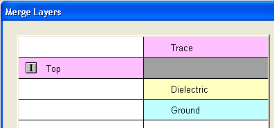
• The dialog shows the object layers on the left and the design layout layers on the right. In the example above, the object has just one layer (Top) while the layout has three layers (Trace, Dielectric, and Ground). • When an object layer is adjacent to a layout layer (the Top and Trace layers in the example above), the M button is displayed, and the layers will be merged. • When an object layer is adjacent to a blank cell on the layout, the I button is displayed, and the object layer will be inserted:
• Clicking on an M or I button toggles the layer between the Merge state and the Insert state. An error occurs if you try to change an Insert layer to a Merge layer when no layers are free for merging. • Click and drag an object layer to a different vertical position. Changing position retains the Merge or Insert state. If an Insert layer is dragged, the layout layers rearrange to leave an empty cell adjacent to the Insert layer. If a Merge layer is dragged, it snaps adjacent to the nearest free layout layer. • Check the Flip Source Layers box to invert the order of the object layers (the order of the layout layers in not changed). This operation can be used, for example, to match the layers of a soldered-on object (signal, solder, assembly) from the top to the bottom of a two-sided board. • When the layer mapping is set up as desired, click the Merge Layers button to execute the mapping. The component is now attached to the cursor for placement in the layout or schematic. • Clicking the Cancel button cancels the placement of the component.
HFSS视频教程 ADS视频教程 CST视频教程 Ansoft Designer 中文教程 |
|
Copyright © 2006 - 2013 微波EDA网, All Rights Reserved 业务联系:mweda@163.com |
|