关于高速CAN总线的PCB layout要点
英文为文档中的原文。
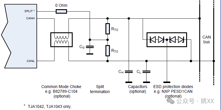
1、When a common mode choke is used, it should be placed close to the transceiver bus pins CANH and CANL
如果节点有共模电感,共模电感应该靠近收发器放置
2、The PCB tracks for the bus signals CANH and CANL should be routed close together in a symmetrical way. Its length should not exceed 10cm.
PCB板上的CANH和CANL走线时应该等长走线,紧耦合,相互靠近;且板上的走线不要超过10cm。
3、Avoid routing other “off-board” signal lines parallel to the CANH/CANL lines on the PCB due to potential “single ended” noise injection into CAN wires
如果PCB上某类走线最终会通过连接器引出到板外,那么在PCB上,CANH和CANL就不要平行于这类走线。
4、The ESD protection should be connected close to the ECU connector bus terminals
ESD器件靠近ECU的连接器端子放置。
5、Place VCC and VIO capacitor close to transceiver pin.
退耦电容靠近收发器的PIN放置。
6、For TJA1051/3 and TJA1042/3: Decouple the VIO pin by a capacitor to VCC (instead GND) close to the transceiver pin to achieve a high-frequent short of the supplies and thus to improve the electromagnetic immunity by enabling the same HF-conditions like existing with VCC connected directly to VIO in 5V-only environments.
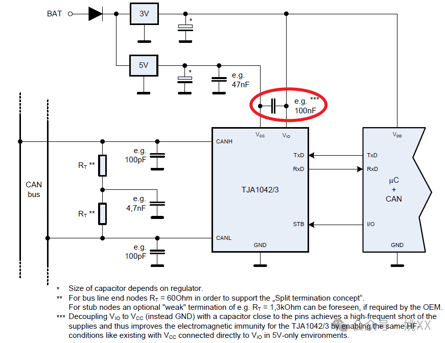
对于有VIO引脚的收发器,如果VCC和VIO是不同的电压,那么它们之间的的耦合电容(图中已标出)应该尽可能的靠近收发器,以实现VCC和VIO之间的高频通路。如果VCC和VIO是同一个电压,VCC和VIO直接连接。
7、The track length between communication controller / μC and transceiver should be as short as possible
CAN的控制器(通常在处理器内部,少部分是独立的)与收发器之间的走线应该尽可能的短。
8、The ground impedance between communication controller (μC) and transceiver should be as low as possible
CAN的控制器的“地”与收发器的“地”的互连应该尽可能的低阻,建议采用完整地平面连接。
9、Avoid applying filter elements into the GND signal of the μC or the Transceiver. GND has to be the same for Transceiver and μC.
CAN的控制器的“地”与收发器的“地”是同一个地,它们之间不要加滤波元件(典型的如磁珠等等)。也不要做成单点互连的形式。
这一条其实和第8条表达的意思本质上相同的。

