|
微波射频仿真设计 |
|
|
微波射频仿真设计 |
|
| 首页 >> Ansoft Designer >> Ansoft Designer在线帮助文档 |
|
Layout Editor User Guide > Drawing a 2.5D Via1. Select a signal or ground layer to draw upon. 2. On the Draw menu, click Via. 3. Select the via’s center point using the mouse or the keyboard. The via is now listed under Model/Vias in the project tree. 4. With a via selected, click Draw > EM Design Properties, or right-click the via and choose EM Design Properties, which brings up the following submenu:
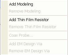
Select Add EM Design Via Properties to open the Via Properties dialog: 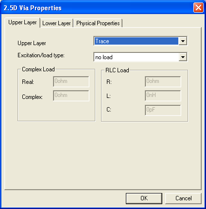 To open the above dialog, you can also select one or more
vias and then right-click on the
Upper Layer Properties 5. Click the Upper Layer tab and do the following: a. Specify the top layer — a signal or ground layer — at which the via terminates. b. If the top layer contains the load, select a load type from the Excitation/Load Type list. You may only define a load at one end of the via. The load on the other end is then set to zero. c. If you selected complex, type the real portion of the complex load in ohms in the Real text box. Then type the imaginary portion of the complex load in ohms in the Complex text box. d. If you selected any RLC combination, do the following: • Type the resistance value in ohms in the R text box. It must be a positive or zero value. • Type the inductance value in nanohenrys in the L text box. It must be a positive or zero value. • Type the capacitance in picofarads in the C text box. It must be a positive value.
Lower Layer Properties 6. Click the Lower Layer tab and do the following:  a. Specify the bottom layer — a signal or ground layer — at which the via terminates b. If the bottom layer contains the load, select a load type from the Excitation/Load c. If you selected complex, type the real portion of the complex load in ohms in the Real text box. Then type the imaginary portion of the complex load in ohms in the Complex text box. d. If you selected any RLC combination, do the following: • Type the resistance value in ohms in the R text box. It must be a positive or zero value. • Type the inductance value in nanohenrys in the L text box. It must be a positive or zero value. • Type the capacitance in picofarads in the C text box. It must be a positive value.
Physical Layer Properties 7. Click the Physical Properties tab and do the following: 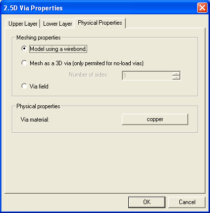 a. Optionally, select Model using a wirebond b. Optionally, select Mesh as a 3D Viaand then choose the number of sides c. Optionally, select Via field d. Click the Via material button at right. The material browser appears. Follow the procedure for assigning a material. 8. Click OK. The via is set at the specified position.
Related TopicsSelecting Load Types for 2.5D Vias
HFSS视频教程 ADS视频教程 CST视频教程 Ansoft Designer 中文教程 |
|
Copyright © 2006 - 2013 微波EDA网, All Rights Reserved 业务联系:mweda@163.com |
|


