|
微波射频仿真设计 |
|
|
微波射频仿真设计 |
|
| 首页 >> Ansoft Designer >> Ansoft Designer在线帮助文档 |
|
HFSS and Planar EM Simulators > Creating a Probe Port
To create a probe port, you follow much the same procedure for creating a 2.5D via, but select coaxial excitation as the Excitation/load type. 1. Select a signal or ground layer to draw upon. 2. On the Draw menu, click Via. 3. Select the via’s center point using the mouse or the keyboard. 4. With a via selected, click Draw > EM Design Properties, or right-click the via and choose EM Design Properties, which brings up the following submenu: 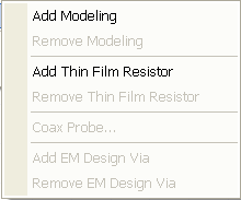 5. Select Coax Probe to convert the via to a coaxial probe. Select Add EM Design Via to open the Via Properties dialog: 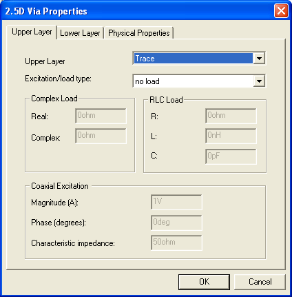 The following controls are available.
Upper Layer Properties 6. Click the Upper Layer tab and do the following: a. Specify the top layer — a signal or ground layer — at which the via terminates. b. Select a load type from the Excitation/load type pulldown menu. If the top layer contains the load, select coaxial excitation as the load type. You may only define a load at one end of the probe. The load on the other end is then set to zero. c. If coaxial excitation is not listed, check whether the coaxial excitation is defined at the other end of the via. If coaxial excitation is not listed at either end of the via then the via needs to be converted to a coaxial probe. d. If you selected complex, type the real portion of the complex load in ohms in the Real text box. Then type the imaginary portion of the complex load in ohms in the Complex text box. e. If you selected any RLC combination, do the following: • Type the resistance value in ohms in the R text box. It must be a positive or zero value. • Type the inductance value in nanohenrys in the L text box. It must be a positive or zero value. • Type the capacitance in picofarads in the C text box. It must be a positive value. f. Type the desired current in amps in the Magnitude text box. Generally, use the default value of 1 mA. This specifies that the solution’s current is scaled in such a way that the excitation current delivers 1 milliamp. To view the solution at another current, enter a positive value. Only modes with non-zero magnitudes are used in post processing. g. Type the phase in degrees. h. Type the characteristic impedance in ohms.
Lower Layer Properties 7. Click the Lower Layer tab and do the following:  a. Specify the bottom layer — a signal or ground layer — at which the via terminates b. Select a load type from the Excitation/load type pulldown menu. If the bottom layer contains the load, select coaxial excitation as the load type. c. If you selected complex, type the real portion of the complex load in ohms in the Real text box. Then type the imaginary portion of the complex load in ohms in the Complex text box. d. If you selected any RLC combination, do the following: • Type the resistance value in ohms in the R text box. It must be a positive or zero value. • Type the inductance value in nanohenrys in the L text box. It must be a positive or zero value. • Type the capacitance in picofarads in the C text box. It must be a positive value. e. Type the desired current in amps in the Magnitude text box. Generally, use the default value of 1 mA. This specifies that the solution’s current is scaled in such a way that the excitation current delivers 1 milliamp. To view the solution at another current, enter a positive value. Only modes with non-zero magnitudes are used in post processing. f. Type the phase in degrees. g. Type the characteristic impedance in ohms.
Physical Layer Properties 8. Click the Physical Properties tab and do the following: 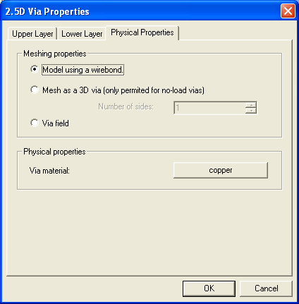 a. Model using a wirebond — Vias are modeled as a wirebond; a single wire element connecting the start and end of the via and intersecting all layers in between. This modeling method is recommended when the diameter of the via is electrically small since it is highly accurate and efficient. Vias used in designs that contain 3D objects will automatically be modeled as two dimensional ribbons. b. Mesh as a 3D Via — Vias are modeled as a ribbon (sides < 3) or a true three-dimensional solid, depending on the number of sides specified. This modeling method (with sides > 2) can be used for vias of any diameter, but may be inefficient if the via diameter is small. — Number of sides: Defines the n-sided prism to use when meshing the via. c. Via field — For a large number of vias filling a region, the Via field option simplifies the field by thinning the vias within each via cluster on a layer. A cluster is defined as a group of vias with roughly the same inter-via spacing. Thinning does not alter connectivity; all geometry connected by a via remains connected. —
Relative min. via spacing: Thinning is based on the minimum average
via d. Click the Via material button at right. The material browser appears. Follow the procedure for assigning a material. 9. Click OK. The probe port is listed under Excitations in the project tree. Double-click the entry in the project tree to edit the probe port’s excitation properties. Aditional properties are available in the Properties window.
Individual settings for a via take precedence over the more general settings described above. The meshing properties of an individual via are set through EM Design Properties. The PlanarEM via properties may be removed from a via without removing the via. Older projects may have existing PlanarEM via properties for all vias. By default, vias no longer automatically receive PlanarEM via properties.When working with a Probe, you can select Draw > Toggle Between Pin and Via to convert the Pin to a Via and then reconfigure the Via settings using the options described in Drawing a 2.5D via.
HFSS视频教程 ADS视频教程 CST视频教程 Ansoft Designer 中文教程 |
|
Copyright © 2006 - 2013 微波EDA网, All Rights Reserved 业务联系:mweda@163.com |
|


