|
微波射频仿真设计 |
|
|
微波射频仿真设计 |
|
| 首页 >> Ansoft Designer >> Ansoft Designer在线帮助文档 |
|
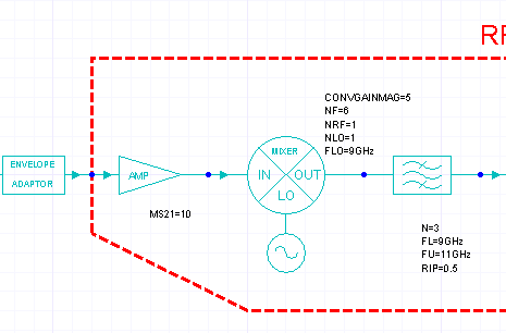
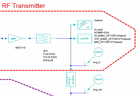
Nexxim Design Examples > RF Transmitter SchematicThe RF transmitter stage takes the I/Q modulated signal as input and outputs the signal mixed with the carrier wave, amplified and filtered. Here is the left side of the RF Transmitter schematic:
This part of the RF transmitter contains the following elements, two from the System nonlinear RF library and one from the Nexxim component library: • An amplifier from the System nonlinear RF library provides a 10dB gain. • A mixer from the System nonlinear RF library mixes the LO frequency (9GHz) with the upshifted data around 1GHz.The mixer adds a conversion gain from RF (in) to IF(out) of 5dB and a noise figure of 6dB. • Athird-order Chebyshev bandpass filter from the Nexxim component library. The filter is set to pass frequencies between 9GHz and 11GHZ with a maximum inband ripple of 0.5dB. Here is the right side of the RF Transmitter schematic:
This part of the RF transmitter contains the following elements, one from the System nonlinear RF library and one from the Nexxim component library: • Another amplifier from the System nonlinear RF library provides a 10dB gain postfilter. • A fifth-order Chebyshev bandpass filter from the Nexxim component library. The filter is set to pass frequencies between 9.5GHz and 10.5GHZ, this time with a maximum inband ripple of 0.05dB. • A system probe, channel, is inserted to enable you to view the output of the RF transmitter. • An adjacent channel power ratio probe, ch_acpr, is inserted to enable you to view the in-band and out-of-band power outputs from the RF transmitter. • An average power probe, avg_in, is inserted to enable you to view the average output power from the RF transmitter.
HFSS视频教程 ADS视频教程 CST视频教程 Ansoft Designer 中文教程 |
|
Copyright © 2006 - 2013 微波EDA网, All Rights Reserved 业务联系:mweda@163.com |
|