|
微波射频仿真设计 |
|
|
微波射频仿真设计 |
|
| 首页 >> Ansoft Designer >> Ansoft Designer在线帮助文档 |
|
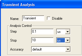
Nexxim Design Examples > Perform a Transient Analysis of the InverterWe must add a solution setup before we can analyze the inverter circuit. 1. On the Circuit menu, click Add Nexxim Solution Setup > Transient Analysis. 2. A window opens for you to specify the parameters for the transient analysis. 3. Set the Step value to 0.1 microseconds, using the pulldown menu to select the unit (us). This is the maximum step size. 4. Set the Stop value to 10 microseconds (us), to define the length of the simulation. Since the frequency of the input sinusoid is 1 MHz, ten microseconds should contain ten cycles. The Analysis Control panel should look like the following:.
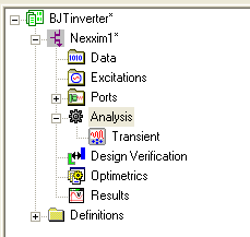
5. On the Transient Analysis window, click OK. 6. Click on the Project tab of the Project Manager, and expand the project icon by clicking on the plus sign. Expand the Nexxim1 icon, then the Analysis icon. You will see the solution setup you just created, named Transient if it is the first, or Transientn for the nth one you create.
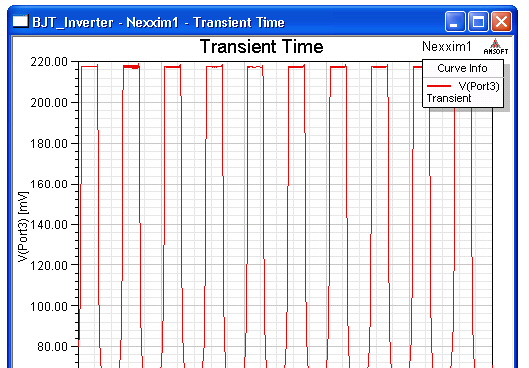
7. Left click on that solution setup to select it, then right click to display a pulldown. From that pulldown, click Analyze (or click the Analyze icon on the toolbar). A progress window briefly appears at the lower right to indicate that the transient analysis is being performed. When the analysis is completed, the Message Manager window at the lower left shows the name of the project, errors or warnings if any, and analysis statistics such as CPU time. 8. In the Project window, locate the Results icon. Right click on the Results icon, then select Create Standard Report > Rectangular Plot. 9. The Create Report dialog opens with the Trace tab selected. The X-axis will display the time values. For the Y-axis, select Voltage as the Category, V(Portn) as the Quantity, and <none> as the Function. NOTE: The Port number (Port3 in our example) and the other node names (net_n) may have different numbers in your circuit. However, there should be only one port voltage to select. 10. Click New Report. 11. Click Close on the Report dialog box. 12. The Reports window displays the graph of the result:
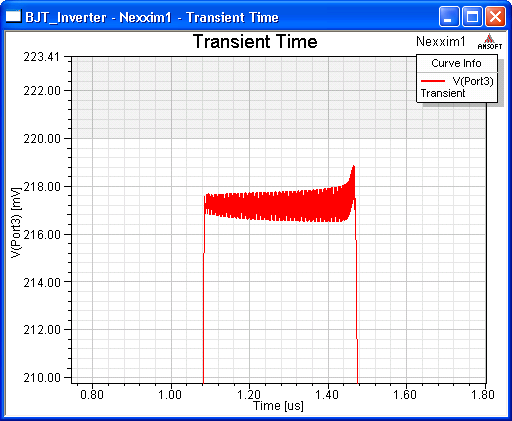
The BJT inverter has converted the sinusoidal input to a square wave output. Note the slightly ragged appearance at the peaks of the wave. Let us look more closely at one of these segments. 13. Right-click anywhere in the Reports window, then select View > Zoom In from the pulldown that displays. Left-press directly above and to the left of one of the wavetops, then hold the button down while you slide the cursor down and to the right to include the wavetop. Release the mouse button. The graph changes to show the zoomed-in view. NOTE: To restore the full image (not zoomed in), right-click in the graph, then select Fit All from the pulldown. 14. You may have to repeat this operation once or twice more until you see an image like the following:
This tiny irregularity (approximately 1.0 mV) is called “trapezoidal ringing.” It is produced by the trapezoidal rule method of numerical integration, and is not the true circuit behavior. The trapezoidal rule is Nexxim’s default numerical integration method. Numerical ringing commonly occurs with the trapezoidal rule method at points in a waveform with sharp corners or discontinuities such as this square wave. 15. Leave the Reports window open with the zoomed-in trace.
HFSS视频教程 ADS视频教程 CST视频教程 Ansoft Designer 中文教程 |
|
Copyright © 2006 - 2013 微波EDA网, All Rights Reserved 业务联系:mweda@163.com |
|