|
|
|
| 首页 >> CST教程 >> CST2013在线帮助系统 |
Waveguide Port
|
|
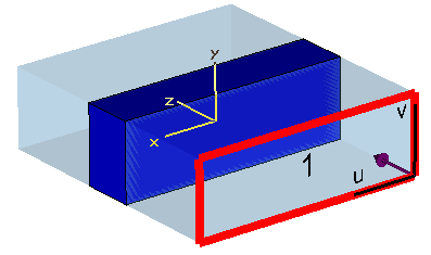
Note: When defining a new port, or when selecting an old one, the local coordinate system of the port, which is determined by the orientation of the global coordinate system, is displayed in the main view. In addition, an arrow indicates the chosen radiation direction if the port is excited. |
|
Text size: Use this slider to adjust the text size of the port number in the main-view.
Position frame
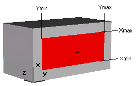
Coordinates: Here, you may choose different possibilities for entering the transversal port dimensions as well as its normal position.
|
|
|
|
|
|
Free normal position: Please activate this button to define an internal port, i.e. a port location inside the calculation domain. This check button is only enabled for a Free or Full plane transversal range setting (see above).
|
The value for the normal position can be inserted in the corresponding X/Y/Zpos text field. Note: Deactivating this button will always locate the port on the lower or upper boundary of the calculation domain, corresponding to the definition of the lower or upper port orientation. |
|
Reference plane frame
Distance to ref.
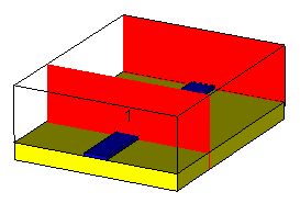
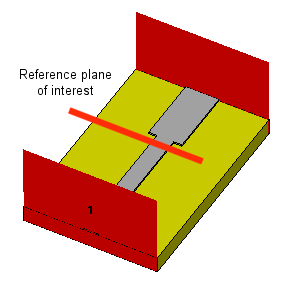
plane: Specifies the distance to your reference plane to obtain
the correct phase information for the S-parameters (deembeding). Positive values move the reference
plane outwards, negative inwards.
The deembeding
can also be performed after the calculation run. See Postprocessing:
Signal Post Processing
![]() S-Parameter Calculations
S-Parameter Calculations ![]() Deembed S-Parameter.... The picture
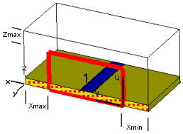
below shows a waveguide port with negative distance to the reference plane,
i.e. the reference plane is moved inwards.
Deembed S-Parameter.... The picture
below shows a waveguide port with negative distance to the reference plane,
i.e. the reference plane is moved inwards.
Mode settings frame
Multipin port: Check this box if you want to define a multipin port.
Define pins...: After you press this button, the Current Set Definitions Dialog will appear and you may define a multipin port by adding new current sets. On leaving the dialog, the Multipin port check box will be checked or unchecked, depending on the existence of multipins.
Number of modes: Specifies the number of modes to be calculated and used for the simulation.
Single-ended: This check button offers the possibility to automatically recalculate the scattering parameters as a post processing step due to previously defined single-ended multipin ports. Consequently during setup of the multipin definition a separate mode set has to be created for each of the inner conductors, i.e. one (usually the outermost) conductor remains undefined representing the ground conductor. Afterwards this check button is enabled and can be activated for single-ended calculation.
For more detailed information about single-ended ports please refer to Multipin Port Overview.
Please note, that by applying single-ended port mode calculation the solvers automatically activate renormalization to fixed impedance, however, the impedance value itself can be modified in the corresponding solver dialog box before starting the simulation.
Ensure shielding: If the port mode domain is not already electrically shielded (as e.g. in a coaxial waveguide) this box can be checked to activate a special treatment of the boundary:
electric: the boundary of the waveguide port is treated as a PEC shielding frame.
magnetic: the boundary of the waveguide port is treated as a PMC shielding frame. Note that conductors in the port shield will not be removed and might cut through the PMC shield.
Leaving this box unchecked will apply the default treatment for port boundaries of the used solver.
Impedance and calibration: Check this box if you want to define impedance, calibration and polarization lines. More detailed information about mode calibration is given in the Waveguide Port Overview.
Define lines...: Pressing this button will open the Mode Impedance and Calibration dialog box enabling you to define impedance, calibration and polarization lines. On leaving the dialog, the Impedance and calibration check box will be checked or unchecked, depending on the existence of data.
Please note: Definition of impedance and calibration lines is currently only available for tetrahedral mesh representations.
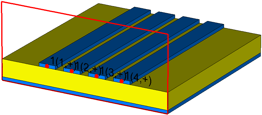
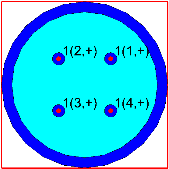
Polarization angle: When mode degeneration occurs, two modes sharing one propagation constant can be combined linearly. By entering a polarization angle (between 0 and 360 degrees) you can determine the main direction of the E-fields for the first of those modes, which will then be visualized by a green arrow in the port plane:
![]()
A more detailed description can be found on
the Waveguide
Port Overview page.
Please note that the usage of the polarization angle is only available
for the first set of degenerated modes and in case that the
Impedance and Calibration check box is not enabled.
OK
Accepts your settings and leaves the dialog box.
Apply
Stores the currently defined port. The dialog box open remains open.
Cancel
Closes this dialog box without performing any further action.
Help
Shows this help text.
See also
Transient Solver, Frequency Domain Solver, Modeler View
Waveguide Port Overview, Discrete Port,
Multipin Port Overview, Current Set Definitions, Define Current Set Item,
Mode Impedance and Calibration, Adding Impedance and Calibration lines,
Reference Value and Normalization


HFSS视频教程 ADS视频教程 CST视频教程 Ansoft Designer 中文教程
|
Copyright © 2006 - 2013 微波EDA网, All Rights Reserved 业务联系:mweda@163.com |
|