
 Microstrip reference block
This type of block represents a reference block for microstrip lines, junctions, couplers and discontinuities.
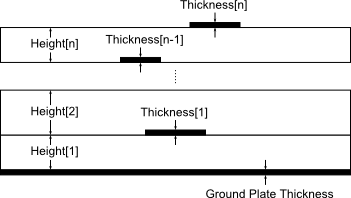
The following figure illustrates the cross-section of microstrip substrates that are supported by this block.

This type of reference block defines all material properties and the vertical dimensions of the substrate. The metallization patterns are defined by the referencing blocks. Typically one referencing block uses only one metal layer, i.e. it defines a metallization pattern on the chosen layer, and the other metal layers remain empty.
The following properties, which describe all cross-sectional properties of microstrip components, including substrate specifications but excluding trace widths, can be defined for this type of reference block. To modify the values, use the Block Properties – Parameters dialog box.
|
Number Of Layers |
Number of dielectric and metal layers. By setting this property to a value greater than 1, arbitrary material stackups can be created. The six properties Height, Thickness, Epsilon, Tandelta, Rho and Roughness offer one value for each layer, counting from bottom to top. Please note that the standard model and the 3D calculation by CST MICROWAVE STUDIO support only a standard microstrip substrate with one layer. The fast 2D EM based model and the enhanced 2D EM based model support up to five layers. The 3D layout view and simulation projects created from it support an arbitrary number of layers. |
|
Height |
Height of the substrate |
|
Thickness |
Thickness of the trace |
|
Epsilon |
Relative permittivity of the substrate |
|
Tandelta |
Dielectric losses |
|
Rho |
Metal resistivity normalized to gold resistivity of 24.4 nΩ m |
|
Roughness |
Roughness of the metal |
|
Ground Plate Thickness |
Thickness of the ground plate |
|
Ground Plate Rho |
Ground plate resistivity normalized to gold resistivity of 24.4 nΩ m |
|
Ground Plate Roughness |
Roughness of the ground plate |
|
Substrate Xmin |
Absolute or relative location of the left substrate edge |
|
Substrate Xmax |
Absolute or relative location of the right substrate edge |
|
Substrate Ymin |
Absolute or relative location of the bottom substrate edge |
|
Substrate Ymax |
Absolute or relative location of the top substrate edge |
|
Absolute substrate dimensions |
The four properties Substrate Xmin, Substrate Xmax, Substrate Ymin and Substrate Ymax are the absolute coordinates of the substrate boundaries if this property is set. Otherwise, they are relative margins between the outermost layout elements and the four substrate edges. |
The five properties Substrate Xmin, Substrate Xmax, Substrate Ymin, Substrate Ymax and Absolute substrate dimensions are not used directly by the referencing blocks. Therefore, these properties do not influence the simulation of the referencing blocks. They specify the substrate size for the 3D layout view and derived simulation projects instead.
Non-ideal ground plates are not supported by the standard model. Please use the fast 2D EM based model, the enhanced 2D EM based model or 3D calculation by CST MICROWAVE STUDIO in the referencing blocks if you want to consider ground losses.
The standard, fast 2D EM based and enhanced 2D EM based models consider metal losses only if both Thickness and Rho are non-zero. Otherwise, the conductors are assumed to be ideal. The fast and enhanced 2D EM based models consider ground losses only if both Ground Plate Thickness and Ground Plate Rho are non-zero. Otherwise, the ground plates are assumed to be ideal.
See also
Block Overview, Microstrip/Stripline Block Properties - Solver, Layout View, Create New Simulation Project - General