Field coupled workflows
As a prerequisite for a field solver coupling, the cable model has
to be prepared accordingly (see Coupling
to 3D field solver). Uni-directional means the data exchange between
circuit simulator and 3D field solver does only happen in one direction,
either the common mode current on the cable is transferred to the 3D field
solver or the common mode voltage along the cable is transferred to the
circuit simulator. The advantage of the uni-directional field coupling
is its robustness and stability. Its disadvantage is that field resonance
effects will not be considered, in contrast to the bi-directional case).
Closed current
loop in 3D field domain
A circuit to 3D field coupling
implies that the set-ups in both domains agree with each other and indeed
most of the settings are done automatically by the program without any
need of interaction by the user. But the loading of the cable terminals
needs special attention, since the circuit domain allows an additional
degree of freedom compared to the 3D field solver when it comes to the
handling of currents at the cable ends.
The figure below shows a Route placed over a ground plane in he 3D
field domain.

The Route includes a single wire and the corresponding set-up in the
circuit domain is shown in the next figure:

The schematic shows a closed current path, which is enabled by the
virtual ground
symbols. A current through the cable terminals will flow (presumed
that the yellow port includes an excitation source) and this contradicts
the corresponding set-up in the 3D field domain, where a current at Node
N1 and Node N2
isn't able to flow, since there is no connection to the ground plane.
Allowing such a set-up would lead to not intended charge accumulation
and to wrong electric and magnetic fields in the 3D field domain.
In order to prevent the user from inconsistent set-ups, the user is
recommended to use the automatic
connection to metallic environment
function, which is featured inside the Route
definition dialog box. After preparing nodes N1
and N2 for the connection possibility
to the metallic environment and a further modeling step (Modeling),
the 3D field domain set-up looks like in the figure below. Two vertical
PEC wires are added by the program which provide a galvanic connection
from the ground plane to the location of node N1
(and N2):

These vertical PEC wires do not automatically connect or short any
terminals from the cable inside the Route! They only provide an possible
connection and this fact can be visualized by activating the Use
differential cable ports inside the Properties
dialog box of the schematic block as shown in the figure below:

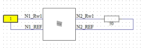
In the schematic two additional pins N1_Ref
and N2_Ref appear. The pins symbolize
the "upper" end of the yellow PEC wires. One can imagine an
infinitesimal short gap between
N1_Rw1 and N1_REF
(and between N2_Rw1 and N2_REF) in the 3D field domain. Now,
closing the connection between N1_Rw1
and N1_REF (and N2_Rw1
and N2_REF) means
to enable the current flow on both sides, in the circuit but also in the
3D field domain.

Note:
For all field coupled workflows the user is recommended
not to use any virtual ground symbols
in the circuit domain. The additional ground pins, provided by the Defining
connection to metallic environment feature prevent the user for setting
up inconsistent simulation projects.
Uni-directional / AC
The uni-directional workflow for the frequency-domain (AC)
differs from the uni- or bi-directional workflows for the time-domain
(Transient). In case of uni-directional / AC the workflow is
separated in two steps: a pure
circuit simulation and a pure 3D field simulation. Both steps communicate
with the help of so called current fieldsources
and voltage monitors. The
order of the two steps depends on whether a radiation
or an irradiation analysis shall
be performed. A radiation analysis
requires a circuit simulation as a first step. Here, the common
mode currents on the cables are calculated and stored inside current fieldsources. In a second step,
the current fieldsources can be taken as a field excitation within the
3D field domain. An irradiation
analysis requires a 3D field simulation first. Here, the tangential
electric field along the cable is calculated and stored in so called
voltage monitors. In a second step these voltages monitors will be taken
as imprinted voltage excitation within the circuit domain.
In order to decide on either the radiation or the irradiation case,
the user has to right mouse click on the schematic block and choose Properties from the pull-down menu.
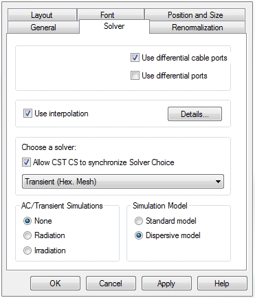
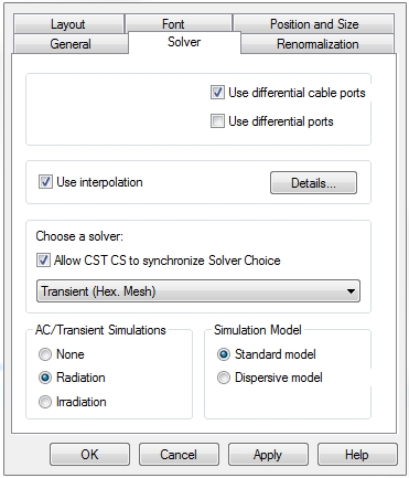
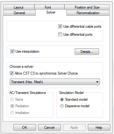
A dialog will appear where the tab Solver
has to be selected:

As solver either Transient (Hex. Mesh)
or Transient TLM (Hex. Mesh) has
to be chosen.
The AC/Transient Simulations
frame allows to decide whether a radiation analysis with the generation
of current fieldsources or a irradiation with the consideration of voltage
monitors shall be performed.
In the Simulation
Model frame the Standard model
interpretation must be chosen. (the Dispersive model is not possible for
any kind of field coupling analysis).
Radiation:
The workflow is strictly separated into two steps. First, an AC-task,
which requires an excitation source, has to be launched in CST DESIGN
STUDIO. It is recommended to use a small number of frequency points only,
since the number of frequency points correlates with the simulation time
for the 3D field simulation. After the AC-task has been finished, the
user has to change into the 3D modeler tab and open the T-solver
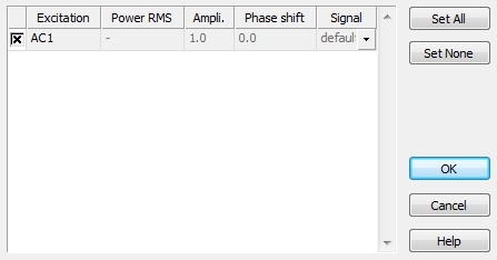
dialog box. The Excitation List
will be automatically filled with the current
fieldsource from the AC-task:

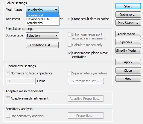
The kind of 3D solver technology can be changed by selecting the corresponding
Mesh type: Hexahedral
stands for FIT, Hexahedral
TLM for TLM. An additional
field source (e.g. a plane wave excitation) can be considered by activating
the Superimpose plane wave excitation
(as shown in the figure below). The simulation starts after pressing the
Start button.

Irradiation:
The workflow is also separated into two steps. First the user has to
set an excitation source (e.g. a plane wave excitation
or an antenna with a discrete port excitation) in the 3D modeler.
The maximum frequency value Fmax
for the 3D field solver is automatically synchronized with the maximum
valid frequency of the cable model (Maximum
valid frequency). In order to chose the 3D solver technology, the
corresponding Mesh type (Hexahedral or Hexahedral
TLM) has to be selected in the T-solver
dialog box (as explained for the Radiation
case, see figure above). After all settings are done the Apply
button has to be pressed, the T-solver
dialog box can be closed and the user has to change to CST DESIGN STUDIO.
Here, the user has to select the irradiation
case in the Solver tab of the
schematic block (right mouse click on the schematic block, choose Properties from the pull-down menu
and select Solver
tab). The irradiation analysis is started by simply launching an AC-task.
The program automatically starts the 3D field solver first and the tangential
electric fields along the cables will be calculated and internally stored
as voltages sources. After the 3D field calculation, the circuit simulation
process starts without any additional interaction from the user. This
automatic connection of the two steps (first step: 3D field calculation,
second step: circuit simulation) has been implemented in order to guarantee
consistent voltage values from the 3D field solver (if a 3D field calculation
could be started independently it could not be guaranteed that the internal
stored voltage values along the cable were consistent to the subsequently
started circuit simulation).
Uni-directional / Transient
In contrast to the uni-directional / AC workflow, the uni-directional
/ Transient workflow is not separated into two steps. The communication
between circuit and 3D field domain takes place on every time step and
doesn't afford any field sources or voltage monitors. The whole simulation
process can be started within a Transient-task from CST DESIGN STUDIO,
regardless whether a radiation or irradiation analysis has to be performed.
The radiation and the irradiation case differ only in the kind of data
exchange: In case of a radiation analysis only the common mode current
on the cable is transferred from the circuit to the 3D field domain. In
case of an irradiation analysis only the voltages along the cable are
transferred from the 3D field to the circuit domain.
The decision on either radiation or irradiation is done with the same
dialog as for the uni-directional / AC case: right mouse click on the
schematic block, choose Properties
from the pull-down menu and selecting the Solver tab:

As solver either Transient (Hex. Mesh)
or Transient TLM (Hex. Mesh) has
to be chosen.
The AC/Transient Simulations
frame allows to decide whether a radiation analysis with the generation
of current fieldsources or a irradiation with the consideration of voltage
monitors shall be performed.
In the Simulation
Model frame the Standard model
interpretation must be chosen. (the Dispersive model is not possible for
any kind of field coupling analysis).
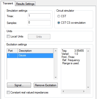
In order to prepare a Transient- task for an uni-directional simulation,
the CST CS co-simulation button
(inside the Circuit simulator
frame) has to be activated as shown in the figure below:

On the 3D field domain side the maximum frequency value Fmax
is automatically synchronized with the maximum valid frequency of the
cable model (Maximum
valid frequency). In addition, the corresponding Mesh
type (Hexahedral or Hexahedral TLM) inside the T-solver
dialog box has been automatically selected according to the selected solver
technology in CST DESIGN STUDIO.
Bi-directional / Transient
From the user point of view the bi-directional/Transient workflow is
almost identical to the uni-directional/Transient case. The communication
between circuit and 3D field domain takes place on every time step and
the whole process can be started within a Transient-task from CST DESIGN
STUDIO. In the bi-directional case, both domains exchange their data simultaneously:
the common mode current on the cable is transferred from the circuit to
the 3D field domain, whereas the voltages along the cable are transferred
from the 3D field to the circuit domain. This simultaneous data exchange
supersedes the distinction between radiation and irradiation. Circuit
and 3D field domain interact and cable-to-field resonances will be considered.
The set-up dialog in CST DESIGN STUDIO (right mouse click on the schematic
block, choose Properties. from
the pull-down menu and select the Solver
tab) recognizes if the cable model is prepared for bi-directional/Transient.
In this case it prevents the user from distinguishing between radiation
or irradiation and the only remaining choice for the user is to select
the 3D field solver technology as it is shown in the figure below:

In the Simulation
Model frame the Standard model
interpretation must be chosen. (the Dispersive model is not possible for
any kind of field coupling analysis).
The remaining steps to set-up a bi-directional analysis are identical
to the uni-directional/Transient case: Inside the Transient-task dialog
box of CST DESIGN STUDIO the CST CS co-simulation
button has to be activated. On the 3D field domain side the maximum frequency
value Fmax is already synchronized
with the maximum valid frequency of the cable model and the corresponding
Mesh type (Hexahedral
or Hexahedral TLM) inside the
T-solver dialog box has also been selected automatically according to
the selected solver technology (see figure above).


