|
微波射频仿真设计 |
|
|
微波射频仿真设计 |
|
| 首页 >> Ansoft Designer >> Ansoft Designer在线帮助文档 |
|
HFSS and Planar EM Simulators > HFSS Setup: Advanced TabClick the Advanced tab of the Add HFSS Solution Setup dialog to access the following settings. 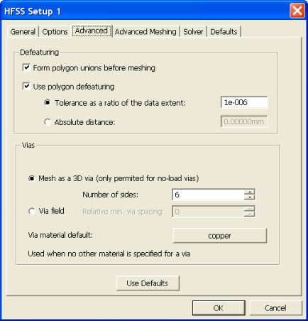 • Form polygon unions before meshing: specifies whether all objects are combined or "unioned" before meshing takes place. This can simplify the mesh; it can, however, also remove internal boundaries that may be desirable. "Unioning" is a complex operation and sensitive to almost coincident edges; it some instances, a union may produce undesirable results. Inspecting the mesh is a simple way to verify the operation. • Use polygon defeaturing: removes very close points, points that don't contribute to the geometry of an edge (e.g. collinear), and very thin intrusions. When used with "unioning", it can be helpful in healing geometry that isn't snapped together. • Tolerance as a ratio of the data exent: tolerance value specified as a ratio of the overall data extent; this value must necessarily be very small. • Absolute distance: tolerance specified as an absolute value, e.g. 0.0001mm • Vias: vias may be modeled as a simple 'wirebond' or as a 3D ribbon or solid. Note: the values specified in the analysis setup only apply to vias that do not have specific property overrides; all properties explicitly specified for a via take precedence over these values. • Mesh as a 3D via: vias are modeled using rectangles to form a 3D ribbon or solid. — Number of sides: number of sides to use when creating the 3D representation; if less than 3, the via is modeled as a flat ribbon. • Via field: it may be possible to reduce the density of via fields and model them using wirebonds without significant loss in accuracy. — Relative min. via spacing: defines a radius around a via; any via that falls within that radius is eliminated. The value specified is a multiple of the average via spacing (the algorithm considers the averages for all via clusters and uses the minimum average spacing). If all vias are spaced equally, then a value of 1 would knock out every other via; a value of 2 would filter out 2 vias between each via. • Via material default: when a material hasn't been specified in the padstack definition and there is no override in the properties for a via, then this will be the material associated with the via mesh.
HFSS视频教程 ADS视频教程 CST视频教程 Ansoft Designer 中文教程 |
|
Copyright © 2006 - 2013 微波EDA网, All Rights Reserved 业务联系:mweda@163.com |
|


