|
微波射频仿真设计 |
|
|
微波射频仿真设计 |
|
| 首页 >> Ansoft Designer >> Ansoft Designer在线帮助文档 |
|
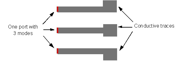
HFSS and Planar EM Simulators > Gap SourcesGap sources represent places in the geometry through which excitation signals enter and leave the structure. The following figure demonstrates the surfaces that have been defined as ports on the edges of conductive traces. Edges on multiple conductors may be defined as a single port with one mode for each conductor. This example has one port with three modes:
A port must lie in a single plane. Ports cannot bend or curve. You may define a port consisting of multiple line segments, but the line segments must lie in the same plane.
The topics for this section include: Including a Length of Uniform Cross-Section Multiple Ports on the Same Face
HFSS视频教程 ADS视频教程 CST视频教程 Ansoft Designer 中文教程 |
|
Copyright © 2006 - 2013 微波EDA网, All Rights Reserved 业务联系:mweda@163.com |
|