关于向CST MWS里导入PCB的问题
大家好:
回家了,终于可以发中文了,版大要是看到了,就把我下面用英文发的那帖子删除了吧:)
最近公司给我一个任务,要我测试一个已投入使用的PCB板的电磁兼容性并给出可行的修改建议。之前我没有用过CST PCB STUDIO, 参考了Help content后开始上手,觉得远没有MWS来的复杂和多变,但是还是有问题出现了。
1:关于把PCB模型导入到PCB时,总显示导入失败(显示文件夹为空),对方公司提供的是用mental graphic expedetion设计的12层PCB板,在查阅贵版的过往帖子时,我看到过一个关于PCB的帖子,说的是好像是大于6层以上的PCB就不能导入PCB STUDIO了,而是要导入MWS,请问是这样的吗?
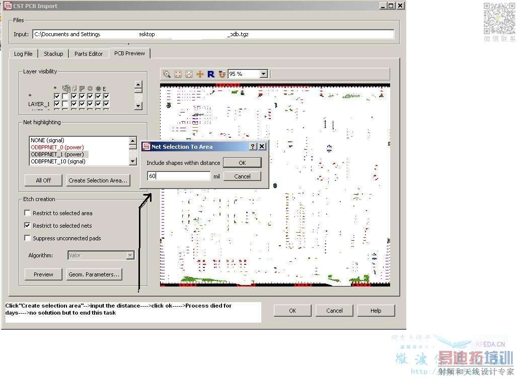
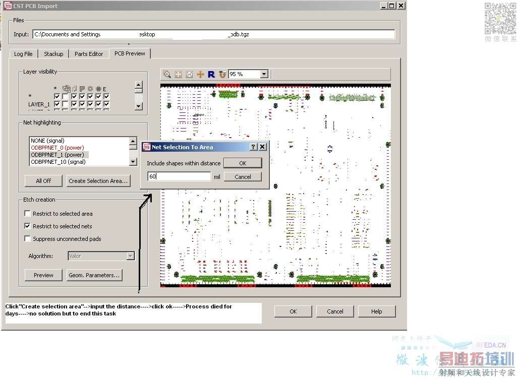
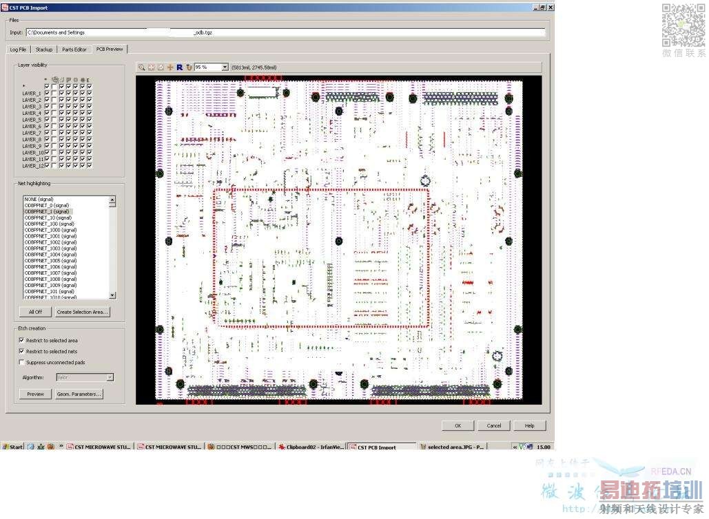
2: 当我导入到MWS时,步骤是MWS-->FILE--->IMPORT--->EDA--->ODB++, 然后这时显示出了PCB文件。大家都知道,为了减少计算时间,在保证精度的情况下,能适当减少mesh数量是一个很好的选择,而在最终导入到working pad前,会有一个选项 :create a selection area, 点击这个后,会出现一个对话框include shapes with distance,此时,我的问题也来了,当我输入一个数值,并点击OK后,CST 就没有响应了,我最长等过一天一夜,还是没有反应。请问大家知道这是为什么吗?另外,大家如果知道如何选取整个PCB的一部分,然后导入的话,请不吝赐教,小弟感谢万分。
为了大家看的更明白,我上传一张图片,劳烦各位啦!
Hi, guys!
Im sorry for explaining my question to you in English because of the my company limitations.. Recently, I've met a problem of importing a PCB (designed by Mental Graphic Expedition )to the CST PCB studio, as the software always warned me with the reason of wrong path and empty folder. Then, I chose to import the PCB model to the CST Micro Wave studio directly and everything was fine until I reached the step of "create a selected area". As everyone knows, to import an entire PCB model to the CST MWS and start the simulation would cost a huge calculation time, and that's why we had such option of reducing the size of PCB model and selecting only the expected area. Ok, when I click "create a selected area" and then a dialog would be poped out and it was "include the distance to the desire trace"(something like that , i cant remember precisely). I inputed a value and click "OK", and now the sofeware would have no response and this situation would last for a day (the longest time i've waited for). I dont know what I've done wrong but if someone here could solve my problem, I would be really grateful!
I will attach a graph of working sheet in order to make my question more clear!
Thank you all guys in advance
12层导入PCBS按理不会出错,你可以在导入的那个界面看一下help,对于很多的格式还是有更具体的要求的。
PCBS没用过,没有建议。
MWS没导入过ODB++格式,参数的解释应该都写在帮助文件里了。
软件停止响应的问题应该只能去问CST技术支持了。
Thank you guys!
The CST German headquarter has sent their contactor to my company just now and these two problems has been solved.
1: About importing the PCB to MWS
He confirmed that it was avaliable to import a PCB with less than 6 layers to the PCB STUDIO for simulations only, and it's better to import it to MWS if you want to do a simulation with a PCB which has more than 6 layers. In my case, the PCB which was designed by Mental Graphic Expedetion should be imported to PCB STUDIO by selecting the path "SIMLAB", NOT "Mental Graphic Expedetion", OR else you can not find the PCB file from the "Mental Graphic Expedetion" folder...
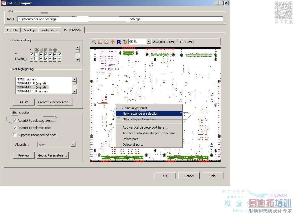
2: When you import the PCB model to the MWS, and if you want to select a small specific area, you should
a: Activate the option "restrict to selected area",
b: Moving your mouse to the PCB graphs showed on the right side and right click,
Now you will see several options. select the option"NEW RECTANGULAR SELECTION", up to now, you can hold the left click and drag the mouse right side down to choose the area you want. (Right click on the other parts outside of the selected area to deavtivate the selected area)
I know it is an individual case which represents little, but I think it is somehow useful if some fresh guys want to use CST to do some simulations of PCB, and sometimes those details of operation are the fundamental steps of using CST. aren't they?:)
Thank you guys again!
There're also graphes for the second question.
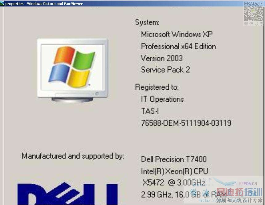
小编的机器什么情况?PCB模型数据多大?
Thanks a lot for your kindly concern, the machine was bought in 2005
500G hard disk, the PCB file (in the form odb++) is 15M
I forgot to attach the graph. In fact, the contactor told me that the machine was good enough to run the CST and bascially the shortage of virtual memory would not happen. He only suggested to run less processes while the simulation was on...
无语ing O__O"…
英语好棒啊,十分羡慕,

