|
微波射频仿真设计 |
|
|
微波射频仿真设计 |
|
| 首页 >> Ansoft Designer >> Ansoft Designer在线帮助文档 |
|
Nexxim Simulator > Bend, Radial

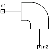
 Netlist FormAxxxx n1 n2 W1=val R=val [ANG=val] n1 and n2 are the names of the nodes attached to the radial bend. The entry COMPONENT=radial_bend identifies the element as a radial bend. The entry SUBSTRATE=substrate_name identifies the microstrip substrate model name selected for the design (see Selecting a Microstrip Substrate). See the Microstrip (MS) Substrate for information on this substrate type.
Netlist ExampleA23 Port1 Port2 W=1e-3 R=1e-6 ANG=75 where FR4, the selected layout technology or substrate type, has a definition such as: .SUB FR4 MS( H=7.6200e-004 Er=4.4 TAND=0.02 TANM=0 Notes1. [All substrates] This element corresponds to the case where the outer corner of the right-angle bend is mitered at an angle, such that the edges of the cut are on the intersection of the reference planes and the outer edges of the bend. In the case W1=W2, the angle of the cut is 45° and the miter ratio is 0.5. 2. [All substrates] Reference planes coincide with the inside vertex of the corner. 3. [Microstrip] Radiation loss is included if cover is not specified in the substrate definition. References1. Wolff, G. Kompa, and R. Mehran, “Calculation method for microstrip discontinuities and T-junctions,” Electron. Lett., Vol. 8, 1972, pp. 177-179. 2. G. Kompa, and R. Mehran, “Planar waveguide model for calculating microstrip components,” Electron. Lett., Vol. 11, 1975, pp. 459-460. 3. T. Okoshi, Planar Circuits for Microwaves and Lightwaves, Springer-Verlag, Berlin, New York, 1983. HFSS视频教程 ADS视频教程 CST视频教程 Ansoft Designer 中文教程 |
|
Copyright © 2006 - 2013 微波EDA网, All Rights Reserved 业务联系:mweda@163.com |
|