|
微波射频仿真设计 |
|
|
微波射频仿真设计 |
|
| 首页 >> Ansoft Designer >> Ansoft Designer在线帮助文档 |
|
Getting Started with Ansoft Designer > Insert Layers1. Access the Stackup tab of the Edit Layers dialog box by doing either of the following: • On the Layout menu, select Layers. • On the Layout toolbar, click
the Stackup dialog icon 2. Insert an infinite ground layer: a. In the Stackup tab of the Edit Layers dialog box, right click in the center of the dialog and select Insert Ground Layer Below. b. In the Name column, change the name to “g1”. 3. In the Stackup tab of the Edit Layers dialog box: a. Right click on the “g1” layer and choose Insert Dielectric Layer Above. b. In the Name column, change the name to “d1”. 4. In the Stackup tab of the Edit Layers dialog box, change the thickness of d1 to 1.5 mm. 5. Insert a trace layer by doing the following: a. In the Stackup dialog box, right click on the dielectric layer and choose Insert signal Layer Above. b. In the Name column, change the name to “t1”. 6. If the stackup created is not in the correct order, you can rearrange it by selecting and dragging the selection handle in the left-most column using the mouse. Select and drag layer t1 above the dielectric layer. The Stackup tab of the Edit Layers dialog box should now look similar to the following:
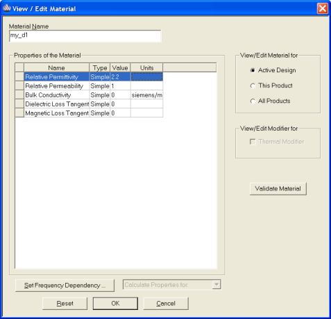
Next, create a new dielectric material and assign it to d1: 1. In the Stackup tab of the Edit Layers dialog box, locate the d1 row, and click the Rogers RT/duroid button. The Select Definition dialog box appears. 2. Click Add Material. The Edit Material dialog box opens. 3. For Material Name, enter “my_d1”, and as the Value for Relative Permittivity, enter 2.2. 4. Make sure Active Design is selected for this material. Leave all other settings unchanged.
5. Click OK to close the Edit Material dialog, and click OK to close the Select Definition dialog. The Stackup tab of the Edit Layers dialog box should now look similar to the following:
6. Click Apply and Close to close the Edit Layers dialog box.
HFSS视频教程 ADS视频教程 CST视频教程 Ansoft Designer 中文教程 |
|
Copyright © 2006 - 2013 微波EDA网, All Rights Reserved 业务联系:mweda@163.com |
|