|
微波射频仿真设计 |
|
|
微波射频仿真设计 |
|
| 首页 >> Ansoft Designer >> Ansoft Designer在线帮助文档 |
|
HFSS and Planar EM Simulators > Stackup Tab ControlsIn the Edit Layers dialog, select the Stackup tab. This opens the Edit Layers Stackup dialog: 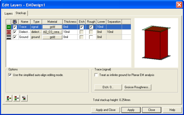
You can now edit the layout or footprint stackup definition. • Use the Add Layer, Remove Layer and Import Stackup buttons on the toolbar to add and remove layers or to import a stackup definition from an XML file. For more information about importing a stackup definition, see Importing a Stackup. • Right-click on any row of the stackup spreadsheet to bring up a menu to insert the various layer types above or below the selected row or remove the layer. • Right-click any column heading to configure which columns are displayed • Click in any cell to edit its contents • Click Model as Ground to model a signal layer as a ground plane (Available in both Simplified and Advanced Stackup Modes). For more information see Model Signal as Ground Plane. • Apply your changes while keeping the Edit Layers dialog open or click Apply and Close to save your changes and close the dialog. • If you click Close before applying the changes you have made, a dialog will open that asks if you would like to apply the changes that were made.
Stackup Modes The Stackup dialog has two modes of operation: Simplified and Advanced.
Simplified Stackup Mode In simplified mode you can only edit the thicknesses of the signal and dielectric layers. The lower elevations/separations between adjacent signal layers is shown for reference but are not editable. The layers can be reordered by dragging and dropping the rows in the stackup spreadsheet. The elevations of signal layers can overlap but, in general, simplified mode is used to create traditional "pancake-style" stackups with strictly alternating signal and dielectric layers.
Advanced Stackup Mode In advanced mode you can manually adjust layer thicknesses, elevations, and drag mode to create very complex stackups. Stackups that have been created in advanced mode may not be compatible with simplified mode and you may not be able to switch between the modes. The advanced options that are available in this mode include: • Drag mode allows you to snap the top, middle, or bottom elevation of a signal layer to a dielectric interface. • Maintain consistent elevations and ordered layers causes the stackup dialog to automatically sort the layers by elevation (for display purposes in the spreadsheet). This option is most often used when editing highly complex stackups that contain manually edited elevations. Note that the actual elevations are not changed by this option. • Treat as infinite ground for PlanarEM analysis (signal layers only) will cause the selected signal layer to be modeled as an infinite ground in the PlanarEM field solver. • Via layer (signal layers only) will treat any objects on the layer as vias — objects that are meshed differently than other objects in the design for improved simulation efficiency. You can control how objects on via layers are meshed by using the Advanced tab of the EM Simulation Setup dialog. For example, you may wish to define a via layer — after importing a GDSII or DXF file that contains a layer with many small circles that define a large number of vias — so that the vias are meshed in an efficient manner. To do this, first set the following properties on the Edit Layers dialog for the layer: layer thickness, material properties, and the "via layer". Next, go to the Advanced simulation options on the Setup dialog for the design and select whether to mesh these objects as wirebonds, simplified 3D objects, or as thinned via fields. • Roughness (signal layers only) allows you to enter the RMS surface roughness for the layer.
The HFSS Etch Factor is specified in the Stackup tab of the Edit Layers dialog. If the Etch column check box for a layer is checked, then the etch factor for that layer will be used when the mesh is created. The Etch button opens the following dialog that can be used to calculate an etch factor based on layer thickness. 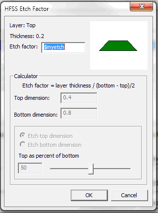 The purpose of the HFSS Etch Factor calculator is to give you a way to calculate an etch factor based on the layer thickness. • When the calculator opens, it is populated with top and bottom dimensions that correspond to the default etch factor, however, the dimension values are representational and do not correspond to a particular geometry in the layout. • The etch factor value may be entered as a number or may be parameterized as a project variable — if the input to that control is a number, the calculator controls are available, otherwise the calculator controls are disabled. The top and bottom dimensions can be changed directly using their edit controls or they can be modified using the slider. The slider sets the value of one dimension to a percentage of the other. As the top and bottom dimensions are changed, both the etch factor and the layer drawing are modified to reflect the change. When the dialog closes, the etch factor is applied to the selected layer.
The Surface Roughness is specified in the Stackup tab of the Edit Layers dialog. By default, Designer layers do not have roughness — but if the Rough column check box for a layer is checked, then the surface roughness for that layer will be used when the mesh is created. The Groisse Roughness button opens the following dialog that can be used to select a surface roughness model. 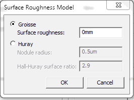 Use the Surface Roughness Model controls to choose between Groisse Surface roughness and Huray. When Huray is selected, you may set the Nodule radius and Hall-Huray surface ratio.
HFSS视频教程 ADS视频教程 CST视频教程 Ansoft Designer 中文教程 |
|
Copyright © 2006 - 2013 微波EDA网, All Rights Reserved 业务联系:mweda@163.com |
|


