|
微波射频仿真设计 |
|
|
微波射频仿真设计 |
|
| 首页 >> Ansoft Designer >> Ansoft Designer在线帮助文档 |
|
HFSS and Planar EM Simulators > Model Signal As Ground PlaneDesigner allows you to model a signal layer as a ground plane. First, access the stackup definition of a component that has been placed in the Layout Editor by selecting Layout Stackup from the Schematic pull-down menu. This opens the Edit Layers dialog. Next, select the Stackup tab, which opens the Edit Layers Stackup dialog. When selected, the Model as Ground option of the Edit Layers Stackup dialog allows you to model a signal layer as a ground plane.
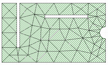
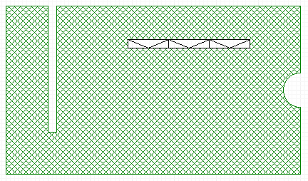
The following diagrams illustrate the difference when a signal layer is modeled as a ground plane.
Modeled as a Signal Layer
Modeled as a Ground Layer
HFSS视频教程 ADS视频教程 CST视频教程 Ansoft Designer 中文教程 |
|
Copyright © 2006 - 2013 微波EDA网, All Rights Reserved 业务联系:mweda@163.com |
|