|
微波射频仿真设计 |
|
|
微波射频仿真设计 |
|
| 首页 >> Ansoft Designer >> Ansoft Designer在线帮助文档 |
|
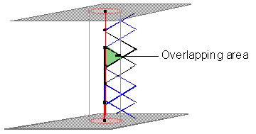
HFSS and Planar EM Simulators > Probe PortsA probe port represents a coaxial A probe source can be defined on any metal layer above or below a ground plane and can pass through multiple layers with or without intervening metal layers. As such, they have a finite radius. The current is assumed to be flowing on the surface of the wire; therefore, the wire’s diameter determines the wire’s inductance and the final results. To mesh this wire, Designer divides the wire into line segments, then creates the mesh from them, as shown below. The current along each line segment is computed using the overlapping regions of the surrounding triangles.
To place an incident field on the source, a frill of magnetic current is applied to the bottom of the probe. The source must be located on a finite or infinite ground plane. The signal travels from the excitation layer in the direction the probe extends. In modeling the probe port, Designer does not assume that the current is constant along the probe wire. Multiple basis functions are used on the probe wire to model the current distribution accurately. The effects of probe current on far-field radiation are calculated.
HFSS视频教程 ADS视频教程 CST视频教程 Ansoft Designer 中文教程 |
|
Copyright © 2006 - 2013 微波EDA网, All Rights Reserved 业务联系:mweda@163.com |
|