|
微波射频仿真设计 |
|
|
微波射频仿真设计 |
|
| 首页 >> Ansoft Designer >> Ansoft Designer在线帮助文档 |
|
HFSS and Planar EM Simulators > DeembeddingDeembedding means adding or subtracting transmission line. In Designer, the Deembed Gap Port Inductance option is only available with HFSS solution setups and gap ports. This section shows an example where subtracting transmission line can be useful and an example where adding transmission line can be useful. The next sections show When HFSS Needs Port Calibration in deembedding and S Matrix Calculation from the Series Impedances to be Deembedded. Consider the aperture-coupled patch antenna shown in Fig. 1. A microstrip trace located below a ground plane feeds a patch antenna located above the ground plane. A slot in the ground plane couples power from the microstrip trace to the antenna. 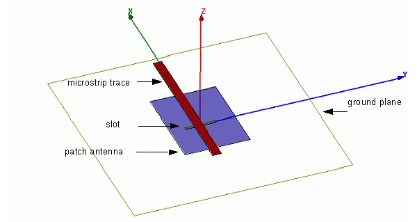 Fig. 1 Aperture-coupled patch antenna
A port is located at the beginning of the trace. It cannot be located very close to the slot, since a port has to be located in a position where a clean transmission-line mode is expected, at some distance from the first discontinuity. The port is shown in Fig. 2. One edge coincides with the ground plane. The other edges are such that the port width is several times the trace width and the port height several times the substrate thickness. The red arrows represent the port field solution. Notice that the three non-ground-plane edges don't influence the port solution noticeably, so this port is large enough. 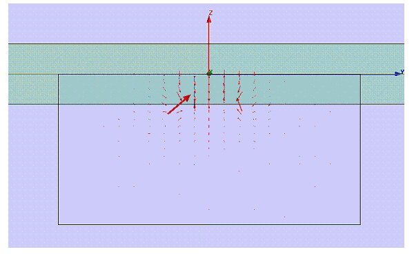 Fig. 2 Magnitude of S11 in dB
The S-parameter characteristic is shown in Fig. 3 in a rectangular plot and in Fig. 4 in a Smith chart. Note that the resonance frequency in Fig. 3 corresponds to the point in Fig. 4 where the curve is closest to the center of the chart. Also note that the curve circles the chart several times. 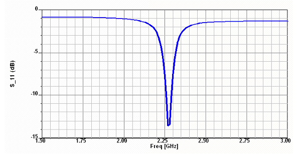 Fig. 3 Magnitude of S11 in dB
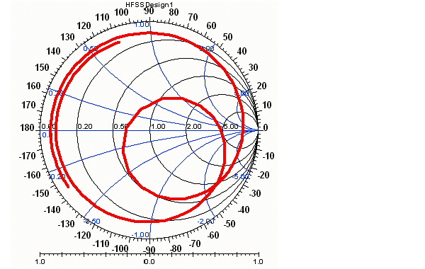 Fig. 4 Smith Chart before deembedding Antenna designers who need to design a matching circuit close to the feed point may want to see the Smith chart with the reference point located close to the feed point of the antenna, that is. close to the slot, rather than some distance away from the feed point. That can be achieved by deembedding. Fig. 5 shows the Smith chart after deembedding.
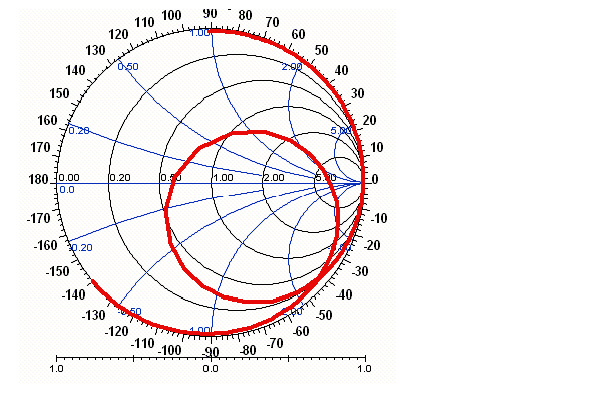 Fig. 5 Smith Chart after deembedding Note that after this kind of deembedding, where transmission line was removed, the curve circles the Smith chart fewer times. As an example where adding transmission line may be useful, consider an IC package or a connector mounted on a printed circuit board. Fig. 6 shows a connector on a printed circuit board. The connector designer has included short sections of traces on the board in his model. These are coupled differential lines, and because of the coupling they share one port. Again, there is some distance between the port and the first discontinuity, so the fields that reach the port form clean transmission-line modes. To model the connector accurately, this model is sufficient.
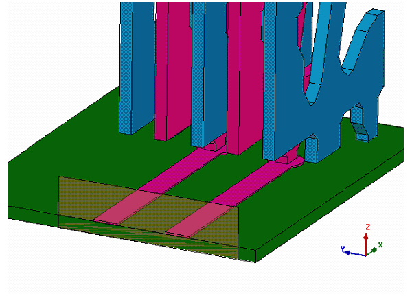 Fig. 6 Connector on printed circuit board On the board, the traces may continue as uniform transmission lines for some distance. To evaluate system performance, it may be desirable to include that length in the S-parameters that are to be exported to a circuit simulator. With deembedding, uniform transmission line can be added as a matrix post processing step. Another example where adding transmission-line length through deembedding may be useful is modeling long cables with frequency-dependent materials, for example, in back planes. In HFSS, only a short section would be modeled, and its behavior over the entire frequency range analyzed accurately. Analyzing only a short section has the benefits of both speed and accuracy. Then, with deembedding, the cable can be extended to any desired length. The S-parameters for the full length can be exported to a circuit simulator to be incorporated into a system.
HFSS视频教程 ADS视频教程 CST视频教程 Ansoft Designer 中文教程 |
|
Copyright © 2006 - 2013 微波EDA网, All Rights Reserved 业务联系:mweda@163.com |
|


