|
微波射频仿真设计 |
|
|
微波射频仿真设计 |
|
| 首页 >> Ansoft Designer >> Ansoft Designer在线帮助文档 |
|
HFSS and Planar EM Simulators > Creating Pin-Based PortsTo create a new pin: 1. Click Draw > Pin and place the pin at the desired location in the Layout Editor. 2. Set the Padstack Definition or Usage in the Footprint Properties. Clicking Padstack Definition will open the padstack definition library where you can select a different pre-defined padstack. Clicking the Padstack Usage button will open the Padstack Editor where you can modify the padstack used by this pin. 3. Select the terminal Location by setting the Pad port layer. The Pad port layer selection will not be displayed if the padstack has no pads. Click the Padstack Usage button to adjust the padstack if desired. 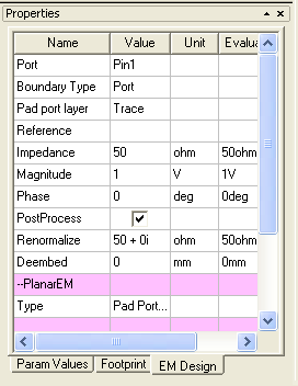
The topics for this section include:
HFSS视频教程 ADS视频教程 CST视频教程 Ansoft Designer 中文教程 |
|
Copyright © 2006 - 2013 微波EDA网, All Rights Reserved 业务联系:mweda@163.com |
|


