|
微波射频仿真设计 |
|
|
微波射频仿真设计 |
|
| 首页 >> Ansoft Designer >> Ansoft Designer在线帮助文档 |
|
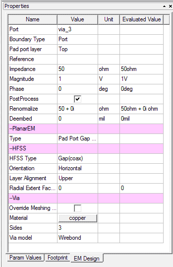
HFSS and Planar EM Simulators > Configuring Pin-Based PortsThe following settings apply to pin-based ports.
— EM Design Properties — • Pad port layer: Sets the terminal location and pad-geometry used for derivation of the HFSS port. • Reference: If applicable, choose the geometry or layer for vertical constraint. • HFSS Type: Either Gap or Gap(coax). • Gap: — Orientation (read only) — Layer Alignment: If applicable, choose layer surface for port-geometry. • Gap(coax) — Orientation (read only) — Layer Alignment: If applicable, choose layer surface for port-geometry. — Radial Extent Factor: Sizing parameter for port-geometry radius.
HFSS视频教程 ADS视频教程 CST视频教程 Ansoft Designer 中文教程 |
|
Copyright © 2006 - 2013 微波EDA网, All Rights Reserved 业务联系:mweda@163.com |
|


