|
微波射频仿真设计 |
|
|
微波射频仿真设计 |
|
| 首页 >> Ansoft Designer >> Ansoft Designer在线帮助文档 |
|
Nexxim Simulator > Voltage Source, Digital Random Bit Generator with Jitter
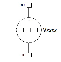 Random Bit Generator Voltage Source with Jitter Netlist FormatThe format for a pseudorandom bit generator voltage source with user-definable jitter is: Vxxxx n+ n- RBG=3 [VTH=val]
[TD=val] [ROUT=val] n+ and n- are the positive and negative nodes.
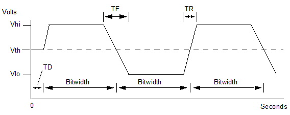
Bit Generator Voltage Source with Jitter Netlist ExamplesV23 23 33 RBG=3 VLO=0 VHI=3 JITTER=1 V43 43 53 RBG=3 VLO=0 VHI=3 JITTER=1 SEED2=1023 In the first example (V23), a random bit sequence is generated with random jitter starting from an internally-generated (pseudorandom) seed. In the second example (V43), the random jitter starts from the given SEED2, and so will be the same each time the simulation is run. Notes1. The RBG source is a time-domain element, suitable primarily for transient analysis simulations. The RBG source can be used in harmonic balance analysis only when a BITLIST is given. See Using the RBG Source with Jitter in Harmonic Balance for details. 2. The BITLIST argument is ignored when a file_reference is supplied via the BITFILE argument. 3. When no BITLIST, BITFILE, or TAPS entry is supplied, the RBG voltage source generates a pseudorandom bit sequence, starting from a random seed value. When no BITLIST or BITFILE is present, the optional SEED can be used to control the bit sequence. The SEED must be an integer value (the maximum absolute value is the maximum size of integers on your system). Using the same SEED guarantees that the same sequence of bits will be generated on each simulation. 4. When a BITLIST, BITFILE, or TAPS is supplied, the RBG source generates the specified sequence of 0 and 1 bits, and repeats the sequence until simulation terminates. When a BITLIST, BITFILE, or TAPS is present, any SEED value will be ignored. 5. In all cases, the sequence of generated bits starts after the time delay given by TD, and continues until the stop time (tstop) of the transient analysis is reached. Each bit changes state with rise and fall times given by TR and TF. and bit duration given by BITWIDTH, measured at the threshold voltage level, VTH. 6. When JITTER_REPEAT is set to 1 and a BITLIST is supplied, Nexxim calculates random jitter data for BITWIDTH, VHI, VLO, TR, and TF on the first iteration of BITLIST, then uses the same sets of jitter data on each subsequent repeat of BITLIST. This results in a periodic signal suitable for harmonic balance analysis. 7. The following diagram illustrates the RBG operation for a source defined as: V23 Port1 0 RBG=3 VLO=1 VHI=3 VTH=2 TD=0.5 TR=0.5
TF=1 BITWIDTH=3 .
8. If TD is negative, an error occurs and the source is ignored. 9. If both TR and TF are omitted, TF and TR are set to BITWIDTH/10. 10. If TR is given and TF omitted, TF is set equal to TR. 11. If TF is given and TR omitted, TR is set equal to TF. 12. If TR or TF is negative or zero, an error occurs and the source is ignored. 13. If BITWIDTH is negative or zero, an error occurs and the source is ignored. 14. The JITTER parameter controls the random variations in bitwidth generated for the bitstream. The the optional SEED2 can be used to control the bit sequence. The SEED2 must be an integer value (the maximum absolute value is the maximum size of integers on your system). Using the same SEED2 guarantees that the same sequence of jitter variations will be generated on each simulation. 15. Using an External File The parameter BITFILE =file_reference refers to an external file containing the bit data. See File References in the Nexxim Netlist File Format topic for details. The format of the VRBG data file is: #bitlist Where bitlist is a sequence of 1’s and 0’s without any whitespace. 16. Using the RBG Source with Jitter in Harmonic Balance The RBG VCVS with jitter is primarily a time-domain element, best simulated with a time-domain tool such as transient analysis. The RBG source can be used with harmonic balance analysis only when an explicit BITLIST is provided. With a random sequence, the circuit cannot reach a steady state required for harmonic balance. For harmonic balance analysis, one test tone must be a submultiple or equal to the bit-frequency of the voltage source. To ensure that the desired HB frequency is used with a RBG VCVS source, qualify the source by adding a TONE=frequency entry at the end of the instance statement. That frequency also appears as an argument in the .HB statement. The default bit-frequency is: 1/[(BITWIDTH + [TR + TF]/2) ´ (number of bits in BITLIST)]
HFSS视频教程 ADS视频教程 CST视频教程 Ansoft Designer 中文教程 |
|
Copyright © 2006 - 2013 微波EDA网, All Rights Reserved 业务联系:mweda@163.com |
|