|
微波射频仿真设计 |
|
|
微波射频仿真设计 |
|
| 首页 >> Ansoft Designer >> Ansoft Designer在线帮助文档 |
|
Nexxim Simulator > Voltage Source, Linear Feedback Shift Register
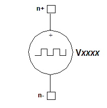 Linear Feedback Shift Register Voltage Source Netlist FormatThe format for a linear feedback shift register voltage source is: Vxxxx n+ n- RBG=5 [VLOW=val]
[VHIGH=val] [TDELAY=val] n+ and n- are the positive and negative nodes. The list_of_taps lists the feedback stages inside brackets and using spaces or commas as separators. The first tap number specifies the number of stages in the device. Subsequent taps must be entered in descending numerical order. Nexxim also accepts the following positional syntax in externally-generated netlists: Vxxxx n+ n- LFSR [(]
vlow vhigh tdlay trise tfall rate seed In this syntax, entries are interpreted by their position in the syntax, left to right.
Linear Feedback Shift Register Voltage Source Netlist ExamplesVLFSR1 node_43 node_53 RBG=5 VLOW=0 VHIGH=1.5 Notes1. If TDELAY is negative, an error occurs and the source is ignored. 2. If TRISE or TFALL is negative or zero, an error occurs and the source is ignored. 3. If RATE is negative or zero, an error occurs and the source is ignored. 4. A SEED value greater than 0.0 is required.
HFSS视频教程 ADS视频教程 CST视频教程 Ansoft Designer 中文教程 |
|
Copyright © 2006 - 2013 微波EDA网, All Rights Reserved 业务联系:mweda@163.com |
|


