|
微波射频仿真设计 |
|
|
微波射频仿真设计 |
|
| 首页 >> Ansoft Designer >> Ansoft Designer在线帮助文档 |
|
Nexxim Simulator > Voltage Source, Clock with Jitter
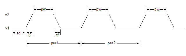
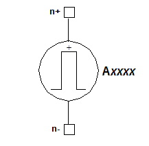 Voltage Clock Source with Jitter Netlist FormatThe format for a voltage clock source with jitter is: Axxxx n+ n- [DC=val]
[V1=val] [V2=val] [TD=val]
[TR=val] n+ and n- are the positive and negative nodes. The entry COMPONENT=vjitter_source is required.
Voltage Clock Source with Jitter ExampleA11 net_1 0 v1=0 v2=1 td=0 tr=1.0e-9 tf=1.0e-9 Notes1. The voltage clock source with jitter is supported only for time domain simulations. 2. Only jitter in the overall clock period is simulated. Pulse width jitter is not calculated separately. 3. The jitter that is simulated is typical of Bounded Uncorrelated jitter (BUJ) rather than true random jitter (RJ). It simulates the jitter due to transitions on neighboring traces, and is uncorrelated with transitions on the clock itself. This device is useful for studies of crosstalk and similar effects. 4. The voltage clock source repeats the clock waveform with random variations in the period. (see diagram below):
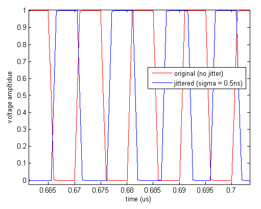
5. If PW is negative, PER and PW are both set to their default values. 6. If nominal period PER is less than (TF+TR+PW), PER is set to (TF+TR+PW) 7. The period is the nominal value set by the PER entry, summed with a jitter value that is drawn at random from a normal distribution using the JITTER entry as the standard deviation. The maximum jitter is plus/minus three standard deviations. The pulse width (V2 hold time) is not affected by the jitter. The optional SEED can be used to initialize the random number sequence. 8. The clock source is a voltage source in series with resistor ROUT. Output resistance ROUT is inserted (internally) at the output of the source. If ROUT is zero, the source is an ideal voltage source. 9. For harmonic balance (HB) analysis, the analyzed tones must be submultiples or equal to the frequencies of the actual voltage or current inputs to the circuit. To ensure that the desired HB frequency is used qualify the source by adding a TONE=tone_val entry at the end of the instance statement. The tone_val is then used in a subsequent HB statement. 10. Here is the time-domain simulation of this example source, showing the clock waveform with and without jitter:
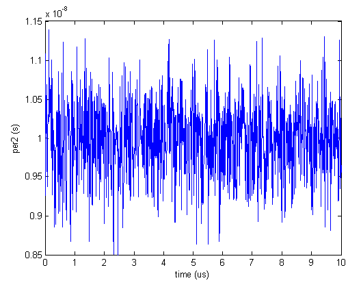
Here is a graph of the period times:
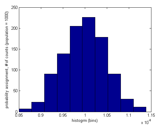
Here is a histogram of the period times:
HFSS视频教程 ADS视频教程 CST视频教程 Ansoft Designer 中文教程 |
|
Copyright © 2006 - 2013 微波EDA网, All Rights Reserved 业务联系:mweda@163.com |
|