|
微波射频仿真设计 |
|
|
微波射频仿真设计 |
|
| 首页 >> Ansoft Designer >> Ansoft Designer在线帮助文档 |
|
Nexxim Simulator > Thin Film ResistorNetlist Format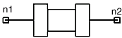 An instance of a coplanar waveguide thin film resistor has the following netlist syntax: ACPWTFRxxx n1 n2 W=val G=val P=val RB=val T=val COMPONENT=cpw_thinfilm_rb SUBSTRATE=substrate_name n1 and n2 are is the names of the nodes attached to the resistor. The entry COMPONENT=cpw_thinfilm_rb identifies the element. The SUBSTRATE=substrate_name is the coplanar waveguide substrate model name selected for the design (see Selecting a Coplanar Waveguide Substrate for details).
Netlist ExampleACPWTFR5 net1 net5 W=0.75e-3
G=1.1e-3 P=2.5e-3 T=1.75e-4 where CPW1, the selected layout technology or substrate type, has a definition such as: .SUB CPW1 CPW( Notes1. A lossy transmission line is used to model the TFR section. Distributed effects are thus taken into consideration. 2. The user needs to define the CPW steps, if any. They are not included in the TFR model.
HFSS视频教程 ADS视频教程 CST视频教程 Ansoft Designer 中文教程 |
|
Copyright © 2006 - 2013 微波EDA网, All Rights Reserved 业务联系:mweda@163.com |
|


