|
微波射频仿真设计 |
|
|
微波射频仿真设计 |
|
| 首页 >> Ansoft Designer >> Ansoft Designer在线帮助文档 |
|
Nexxim Simulator > Coplanar Waveguide Substrate Model
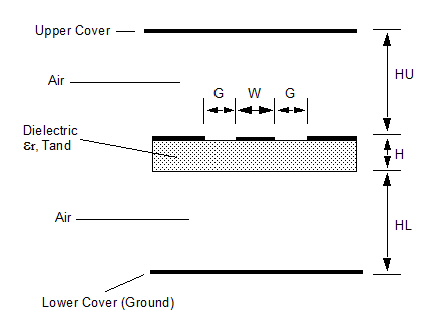
Defining a Coplanar Waveguide SubstrateTo add a new coplanar waveguide substrate definition to an existing design, expand the Project icon, then the Design icon. Right click on the Data icon, and select Add Substrate Definition. The Substrate Definition window appears. Add the substrate name and parameters as desired, then click OK. To edit the definition of an existing substrate, expand the Project icon, then the Design icon, then the Data icon. Click on the icon for the substrate you wish to edit. The Substrate Definition window appears. Add or modify the substrate parameters as desired, then click OK. Coplanar Waveguide Substrate Model Netlist FormatThe Coplanar Waveguide substrate model has the following netlist format: .SUB substrate_name CPW ([H=val]
[HU=val] [HL=val] The substrate_name is the name for the substrate type used in distributed elements that refer to this substrate definition. The entry CPW is required to identify the Coplanar Waveguide substrate type. The CPW identifier must immediately follow the substrate_name. Inside the parentheses, the labeled parameters may be entered in any order.
Coplanar Waveguide Substrate Model Netlist Example.SUB CPW1 CPW(
HFSS视频教程 ADS视频教程 CST视频教程 Ansoft Designer 中文教程 |
|
Copyright © 2006 - 2013 微波EDA网, All Rights Reserved 业务联系:mweda@163.com |
|


