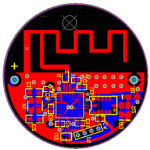

PCB天线对其下方的铺底要求严吗?
我知道四分之一波长天线下面不能有地的,,,你的天线背面肯定也不能有地! 改变距离,天线阻抗肯定改变!
上面那个天线号称可以达到292欧姆的纯阻(2.45GHZ时),但如果铺地靠上或者靠下移动一点,阻抗会变大还是变小呢?
我用ADS的MOMENT仿真了一下,不算最底下那一小段连接端口的线,也只有215欧姆,外加0.0X的容性负载。
刚刚用ADS跑了一下,好象铺地越近电阻越大。但是我做不出很好的铺地效果,只能临时用两块FILL+两个接地符号代替(好象ADS的MOMENT仿真时是要忽略接地符号的?)。我想加两个GROUND REFERENCE型的端口但由于馈电端口时一对DIFFERENTIAL型也用不了。
呵呵,可以设置1 2端口为internal,然后在背面画两块铺底板,分别接3 4端口,ground preference,3是1的相对地,4是2的相对地
The ground will affect the impedance of the dipole. The impedance will increse when the dipole is close to the ground plane. This is similar to the situation of inverted-L/F antennas.
In addition, the effect of the dielectric subtsrate on the antenna impedance is very limited unlike a microstrip antenna.
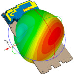
besides the effect of the ground plane on the impedance, the ground plane also affects the radiation patterns along the PCB plane like reflector. Therefore, it is necessary to optimize the spacing between the dipole and ground plane.
the shape of the ground plane also affects the radiation performance indeed.
therefore, you should design the ground plane of a patch antenna carefully.
any more questions?
相关文章:
- sma接口焊接到微带线馈电的时候,还用将sma引脚和介质下方的接地板焊接到一块吗 (05-08)
- 天线基本知识及应用--天线的分类与选择(05-08)
- 关于同轴天线(05-08)
- 广播收听中关于天线的一些基本概念(05-08)
- 智能天线及其应用(05-08)
- 探索智能天线技术(05-08)