转:大牛Prof. Abidi、Prof. Thomas H.Lee高级射频电路课程
05-08
帮转:
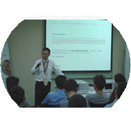
8月26-27日在上海,8月30日在合肥,我们邀请了射频集成电路设计领域专家Prof. Thomas H.Lee, Prof. C. Patrick Yue,以及美国工程院院士、RF CMOS领域权威Prof. Asad A. Abidi为我们带来Advanced RFIC Design的课程,
本课程属于射频集成电路设计高级课程,适合具有一定基础的学员:射频电路、无线通讯等设计人员、模拟/数模混合电路设计人员、器件建模等相关领域的研究人员和管理人员、集成电路专业研究生以及对射频集成电路感兴趣的人。
课程内容:
本课程属于高级射频集成电路设计培训课程,适合具有一定基础的学员:偏重设计中的实际问题,RFIC权威教授:Prof. Thomas H. Lee和Prof. C. Patrick Yue在上海、Prof. Asad A. Abidi在合肥为我们带来以下课程内容:
CMOS RF IC Design
(Prof. Thomas H. Lee, August 26, 2014,Shanghai)
1、Impedance transformation
▲When to do it; When not to do it; how to do it
▲Bode-Fano limits on matching bandwidth
▲Unintended transformation by active circuits: "Strange impedance behaviors (SIBs); simple models and examples
▲Conscious exploitation of SIBs
2、Noise in linear, time-invariant (LTI) systems
▲LNA design: Noise match vs. power match
▲How to use SIBs to achieve good noise and power match simultaneously
▲Noise "cancellation"
3、Noise in linear, time-varying (LTV) systems
▲Phase noise in oscillators: Theory and practice
▲Noise in mixers
4、Nonlinearity
▲Figures of merit: 1-dB compression point; intermodulation intercepts (IP2, IP3); adjacent-channel power ratio (ACPR); spurious-free dynamic range (SFDR)
▲Nonlinearity reduction techniques: Feedback; strong and weak feedforward
5、Techniques for circuit design at extremes of frequency
▲Amplifier bandwidth extension techniques: Shunt peaking; bridged T-coil; distributed architectures; Ft-doubler
▲Oscillator and synthesizer frequency extension techniques: Multiphase push-push-push; frequency multiplication with nonlinear elements; injection locking (if time permits)
▲Power combining structures and strategies: Corporate combiners; free-space combining
▲Interconnect: Microstrip, stripline, coplanar waveguide
Practical RFIC Implementation Techniques in Scaled CMOS Technologies
(Prof. C. Patrick Yue, August 27, 2014,Shanghai)
1、CMOS for RFIC Products
▲Trends in wireless communication and RFIC integration
▲RF technology options: to use or not to use?
▲Scalability of RF CMOS beyond 130nm: device characteristics and passive component quality at RF
2、RF Device and Passive Component Modeling
▲MOSFET macro modeling and layout optimization
▲Physical modeling and layout optimization for inductors
▲Transformer design trade-offs and circuit applications
▲Varactor modeling and optimization – diode vs. MOS
▲Test structure design and characterization techniques
3、 Technology Key Circuit Blocks
▲T/R switch – improve P-1dB and isolation with tuned circuits
▲LNA – topology, sizing and biasing for noise and power
▲Mixer – topology, linearity and noise considerations
▲VCO – phase noise, power and tuning range optimization
4、 Modeling, Substrate Noise and ESD Techniques
▲Methodology for predictable design using RF sub-circuits
▲Supply and substrate noise coupling
▲RF ESD protection strategy from a system perspective
Systematic Design of Oscillator Circuits
(Prof. Asad A. Abidi, August 30, 2014,Hefei)
In this one day tutorial/short course, Prof. Asad A. Abidi will present his unique highly valued training methods and contents of oscillator design based on fundamental analysis and calculation, not the common PDK-based and EDA-based “error-and-try” optimization. It will most benefit circuit designers in industry involved with oscillators and frequency synthesizers.
▲Noise processes in CMOS oscillators;
▲Time-domain jitter calculation;
▲Effects of white noise and flicker noise etc.;
▲What dominates the jitter and phase noise?
▲Where are they arise from?
▲Theocratic analysis and design of circuits with validation;
▲Straightforward expressions for period jitter and phase noise enable manual design;
▲Design guidance from ring and LC oscillator.
有人去听课不?
明天去合肥,上海有人过去吗?
相关文章:
- 射频电路调试需要什么基础?(05-08)
- 关于射频电路天线的磁场问题(05-08)
- 求手机射频电路的资料(05-08)
- 6253平台,用单卡程序下载到双卡的同样射频电路的板子上能搜到卡没信号?(05-08)
- 一本关于射频电路基础理论的书,相当经典(05-08)
- 请教射频电路中splitter这个元件(05-08)
射频专业培训教程推荐


