PCB整板场强分布
05-08
欲仿真PCB的辐射特性,
在CST中具体怎末设置?
最好有简单的例子参考,多谢!
在CST中具体怎末设置?
最好有简单的例子参考,多谢!
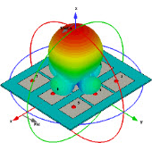
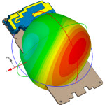
Just establish the PCB model in MWS and treat it as an antenna. Apply the "open add space" boundary condition and add several farfield monitors at the selected frequency points.
板上的元器件不用考虑吗?
Sorry it doesn't make sense to me. Just establish the model as similar as what you gonna to make physically.
相关文章:
- 知道一点的电场强度,能计算出这点的能量吗? (05-08)
- CST中如何计算远区电场强度 (05-08)
- 请问如何知道入射场的场强 (05-08)
- 腔体的Q值及场强分布 (05-08)
- 要仿真一个结构的辐射发射(远场场强)的EMC问题 (05-08)
- CST探针probe如何导出该点电场强度数值形式? (05-08)
射频专业培训教程推荐


