
CPW的来历-这个有趣
05-08
History of Coplanar Waveguide
Coplanar waveguide was invented by Cheng P. Wen. It was invented when Wen was at RCA's Sarnoff Laboratories in New Jersey, way back in 1969, just two years after the Summer of Love. Dr. Wen now lives in Beijing, and continues to pass on his considerable knowledge to microwave engineering students, and he has corresponded with Microwaves101 on the topic of CPW (how's that for name dropping?)
C.P. Wen explains that his original "name" for coplanar waveguide was "planar strip line". A co-worker, Lou Napoli suggested the name coplanar waveguide. Thus with Lou's suggestion, CPW invented CPW!
Types of coplanar waveguide
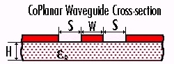
"Classic" coplanar waveguide (CPW) is formed from a conductor separated from a pair of groundplanes, all on the same plane, atop a dielectric medium. In the ideal case, the thickness of the dielectric is infinite; in practice, it is thick enough so that EM fields die out before they get out of the substrate.
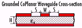
A variant of coplanar waveguide is formed when a ground plane is provided on the opposite side of the dielectric, which is called finite ground-plane coplanar waveguide (FGCPW), or more simply, grounded coplanar waveguide (GCPW).
The advantages of coplanar waveguide are that active devices can be mounted on top of the circuit, like on microstrip. More importantly, it can provide extremely high frequency response (100 GHz or more) since connecting to CPW does not entail any parasitic discontinuities in the ground plane. One disadvantage is potentially lousy heat dissipation (this depends on the thickness of the dielectric and whether it makes contact to a heat sink). However, the main reason that CPW is not used is that there is a general lack of understanding of how to employ it within the microwave design community. I don't want to scare you away from CPW, but a lot of CAD programs don't support it. This will change in the years to come as more millimeter-wave work will demand the benefits of CPW.
Advantages and disadvantages of CPW
In terms of circuit isolation, you can get great isolation using CPW, because there are always RF grounds between traces. Many examples of high-isolation RF switches have used grounded CPW to get 60 dB isolation or more.
The advantage of having a thick substrate is realized when you fabricate CPW MMICs. The expense of backside processing (thinning, via etch, backside plating) is eliminated. Many companies that are currently developing GaN devices are employing CPW so they can concentrate on device technology and not have to figure out how to etch vias in silicon carbide or sapphire. With GaN technology, wafer slices are on the order of 12 mils thick, so for X-band devices, the height of the chip is well matched to 10 or 15 mil alumina.
For GaAs MMICs, wafer slices start out at 25 mils. If a CPW chip is mounted face-up, a severe height discontinuity can result. The way to get around this problem is to use flip-chip technology, which is an advantage or a disadvantage depending on who you talk to!
The ground inductance for shunt elements is quite low for CPW, compared to microstrip applications. This is because the RF ground is "right there", and you don't have to drill a via hole to connect to it (vias add inductance).
As mentioned preciously, if you want to make compact circuits using narrow transmission lines, you must trade off RF loss. CPW circuits can be lossier than comparable microstrip circuits, if you need a compact layout.
In terms of circuit size, CPW is at a disadvantage versus a stripline of microstrip circuit, because it's effective dielectric constant is lower (half of the fields are in air).
Ground straps are always needed to tie the two grounds together in CPW, or weird things can happen. These are especially important around any discontinuity, such as a tee junction.
Unintended spurious transmission modes can also happen. In a parallel-plate mode, the substrate acts like a dielectric-filled waveguide, and EM energy propagates along unintended paths. Don't get us wrong, if you know how to avoid this pitfall, CPW works great!
Coplanar waveguide was invented by Cheng P. Wen. It was invented when Wen was at RCA's Sarnoff Laboratories in New Jersey, way back in 1969, just two years after the Summer of Love. Dr. Wen now lives in Beijing, and continues to pass on his considerable knowledge to microwave engineering students, and he has corresponded with Microwaves101 on the topic of CPW (how's that for name dropping?)
C.P. Wen explains that his original "name" for coplanar waveguide was "planar strip line". A co-worker, Lou Napoli suggested the name coplanar waveguide. Thus with Lou's suggestion, CPW invented CPW!
Types of coplanar waveguide
"Classic" coplanar waveguide (CPW) is formed from a conductor separated from a pair of groundplanes, all on the same plane, atop a dielectric medium. In the ideal case, the thickness of the dielectric is infinite; in practice, it is thick enough so that EM fields die out before they get out of the substrate.
A variant of coplanar waveguide is formed when a ground plane is provided on the opposite side of the dielectric, which is called finite ground-plane coplanar waveguide (FGCPW), or more simply, grounded coplanar waveguide (GCPW).
The advantages of coplanar waveguide are that active devices can be mounted on top of the circuit, like on microstrip. More importantly, it can provide extremely high frequency response (100 GHz or more) since connecting to CPW does not entail any parasitic discontinuities in the ground plane. One disadvantage is potentially lousy heat dissipation (this depends on the thickness of the dielectric and whether it makes contact to a heat sink). However, the main reason that CPW is not used is that there is a general lack of understanding of how to employ it within the microwave design community. I don't want to scare you away from CPW, but a lot of CAD programs don't support it. This will change in the years to come as more millimeter-wave work will demand the benefits of CPW.
Advantages and disadvantages of CPW
In terms of circuit isolation, you can get great isolation using CPW, because there are always RF grounds between traces. Many examples of high-isolation RF switches have used grounded CPW to get 60 dB isolation or more.
The advantage of having a thick substrate is realized when you fabricate CPW MMICs. The expense of backside processing (thinning, via etch, backside plating) is eliminated. Many companies that are currently developing GaN devices are employing CPW so they can concentrate on device technology and not have to figure out how to etch vias in silicon carbide or sapphire. With GaN technology, wafer slices are on the order of 12 mils thick, so for X-band devices, the height of the chip is well matched to 10 or 15 mil alumina.
For GaAs MMICs, wafer slices start out at 25 mils. If a CPW chip is mounted face-up, a severe height discontinuity can result. The way to get around this problem is to use flip-chip technology, which is an advantage or a disadvantage depending on who you talk to!
The ground inductance for shunt elements is quite low for CPW, compared to microstrip applications. This is because the RF ground is "right there", and you don't have to drill a via hole to connect to it (vias add inductance).
As mentioned preciously, if you want to make compact circuits using narrow transmission lines, you must trade off RF loss. CPW circuits can be lossier than comparable microstrip circuits, if you need a compact layout.
In terms of circuit size, CPW is at a disadvantage versus a stripline of microstrip circuit, because it's effective dielectric constant is lower (half of the fields are in air).
Ground straps are always needed to tie the two grounds together in CPW, or weird things can happen. These are especially important around any discontinuity, such as a tee junction.
Unintended spurious transmission modes can also happen. In a parallel-plate mode, the substrate acts like a dielectric-filled waveguide, and EM energy propagates along unintended paths. Don't get us wrong, if you know how to avoid this pitfall, CPW works great!
sharing is good!
文正(C.P.Wen)博士于1969年提出“平面带状线”(Planar strip line),他的同事建议他把该结构的名称改为CPW(coplanar waveguide)。于是,CPW发明了CPW。
这个有意思,谢谢小编发这么好的帖子~
CPW走线原来是这么来的啊~~
really?
thank you!
有意思 原来还有这么一段渊源 学到啦 多谢小编共享 顺带还锻炼英语了 呵呵
看了
yes oh yes oh oh
呵呵,
可能也算巧合,CPW也算好用的.線阻抗可以設計得比MS還要高,以相同功率而言
:9de :9de
以后 可以多一些这样的帖子,培养大家的学习兴趣,了解我们行业的历史
CPW是用哪个软件做出来的? 在ADS中怎么实现? 才开始学习, 有很多不懂, 有没有做过的高手说一下
是挺有意思的
sharing is good!
相关文章:
- 很有趣的电梯心理实验!背朝电梯门的都是实验人员,当进入自然人后,你会有啥反应?(05-08)
- ADS2008U2很奇怪的bug?非常有趣!(05-08)
- 请教一个关于cpw端口设置的问题(05-08)
- HFSS里怎么加CPW馈电?(05-08)
- CST软件CPW馈电时为什么总是报waveport 端口太小(05-08)
- 急~在线等解决!CPW天线实际用馈电头问题(05-08)
射频专业培训教程推荐