
半导体C-V测量基础
05-08
译者按:C-V测试是一个被广泛用于半导体测试的参数,尤其是MOSCAP和MOSFET结构的半导体。其他的一些半导体器件和技术也可以用C-V测量来特征化,包括双极性晶体管,JFETs,III-V 符合器件等。本文会讲到一些C-V测试的的应用和一些定律。
Capacitance-voltage (C-V) testing is widely used to determine semiconductor parameters, particularly in MOSCAP and MOSFET structures. However, other types of semiconductor devices and technologies also can be characterized with C-V measurements, including bipolar junction transistors, JFETs, III-V compound devices, photovoltaic cells, MEMS devices, organic thin film transistor (TFT) displays, photodiodes, and carbon nanotubes.
The fundamental nature of these measurements makes them relevant to a wide range of applications and disciplines. They are used in the research labs of universities and semiconductor manufacturers to evaluate new materials, processes, devices, and circuits. C-V measurements are extremely important to product and yield enhancement engineers responsible for improving processes and device performance. Reliability engineers use these measurements to qualify material suppliers, monitor process parameters, and analyze failure mechanisms.
With appropriate methodologies, instrumentation, and software, a multitude of semiconductor device and material parameters can be derived. This information is used all along the production chain beginning with evaluation of epitaxially grown crystals including parameters such as average doping concentration, doping profiles, and carrier lifetimes.
In wafer processes, C-V measurements can reveal oxide thickness, oxide charges, contamination from mobile ions, and interface trap density. These measurements continue to be important after other process steps such as lithography, etching, cleaning, dielectric and polysilicon depositions, and metallization. After devices are fully fabricated on the wafer, C-V is used to characterize threshold voltages and other parameters during reliability and basic device testing and to model the performance of these devices.
The Physics of Semiconductor CapacitanceA MOSCAP structure is a fundamental device formed during semiconductor fabrication (Figure 1). Although these devices may be used in actual circuits, they typically are integrated into fabrication processes as test structures. Since they are simple structures and fabrication is easy to control, they are a convenient way to evaluate the underlying processes.
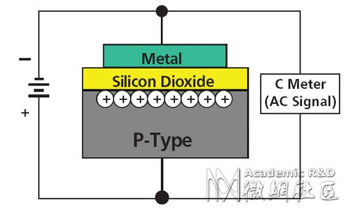
Figure 1. C-V Measurement Circuit for a MOSCAP Structure Formed on a P-Type Substrate
The metal/polysilicon layer shown in Figure 1 is one plate of the capacitor, and silicon dioxide is the insulator. Since the substrate below the insulating layer is a semiconducting material, it is not by itself the other plate of the capacitor. In effect, the majority charge carriers become the other plate.
Physically, capacitance (C) is determined from the variables in the following equation:
k = dielectric constant of the insulator
d = separation of the two plates
As a result, the larger A and k are and the thinner the insulator is, the higher the capacitance will be. Typically, semiconductor capacitance values range from nanofarads to picofarads or smaller.
The procedure for taking C-V measurements involves the application of DC bias voltages across the capacitor while making the measurements with an AC signal (Figure 1). Commonly, AC frequencies from about 10 kHz to 10 MHz are used for these measurements. The bias is applied as a DC voltage sweep that drives the MOSCAP structure from its accumulation region into the depletion region and then into inversion (Figure 2).
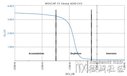
Figure 2. DC Bias Sweep of MOSCAP Structure Obtained During C-V Testing
A strong DC bias causes majority carriers in the substrate to accumulate near the insulator interface. Since they can’t get through the insulating layer, capacitance is at a maximum in the accumulation region as the charges stack up near that interface because d is at a minimum (Figure 1). One of the fundamental parameters that can be derived from C-V accumulation measurements is the silicon dioxide thickness.
As the bias voltage decreases, majority carriers get pushed away from the oxide interface, and the depletion region forms. When the bias voltage is reversed, charge carriers move the greatest distance from the oxide layer, and capacitance is at a minimum because d is at a maximum. From this inversion region capacitance, the number of majority carriers can be derived. The same basic concepts apply to MOSFETs even though their physical structure and doping are more complex.
Many other parameters can be derived from the three regions shown in Figure 2 as the bias voltage is swept through them. Different AC signal frequencies can reveal additional details. Low frequencies uncover what are called quasistatic characteristics where high-frequency testing is more indicative of dynamic performance. Both types of C-V testing often are required.
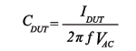
Basic Test SetupFigure 3 is the block diagram of a basic C-V measurement setup. Because C-V measurements actually are made at AC frequencies, the capacitance for the DUT is calculated with the following:
f = test frequency
VAC = magnitude and phase angle of the measured AC voltage
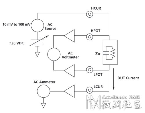
Figure 3. Basic Test Setup for C-V Measurements
In other words, the test measures the AC impedance of the DUT by applying an AC voltage and measuring the resulting AC current, AC voltage, and impedance phase angle between them.
These measurements take into account series and parallel resistance associated with the capacitance as well as the dissipation factor. Figure 4 illustrates the basic circuit variables that can be derived from the measurements.
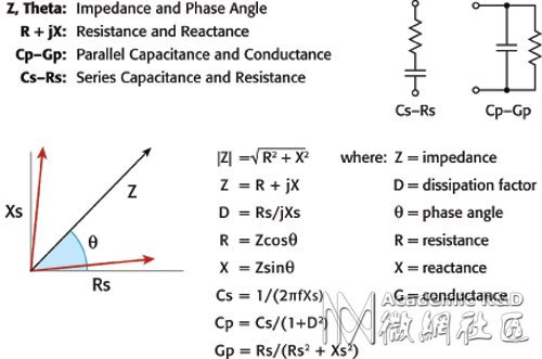
Figure 4. Basic Electrical Variables Available From C-V Measurements
Challenges of C-V MeasurementsAlthough a block diagram of a C-V test setup looks deceptively simple, certain challenges are associated with this testing. Typically, test personnel have problems in the following areas:
• Low-capacitance measurements of picofarads and smaller values
• C-V instrument connections through a prober to the wafer device
• Leaky, high D capacitance measurements
• Using hardware and software to acquire the data
• Parameter extractions
Overcoming these challenges requires careful attention to the techniques used along with appropriate hardware and software.
Low-Capacitance Measurements
If C is small, the DUT’s AC response current is small and hard to measure. However, at higher frequencies, the DUT impedance is reduced so the current increases and is easier to measure.
Often, semiconductor capacitance is less than 1 pF, which is below the capabilities of many LCR meters. Even those claiming to measure these small capacitance values may have confusing specifications that make it difficult to determine the final accuracy in the measurement. If accuracy over the instrument’s full measurement range is not explicitly stated, you need to clarify this with the manufacturer.
C-V Measurement Connections
In most test environments, the DUT is a test structure on a wafer: It is connected to the C-V instrument through a prober, a probe card adapter, and a switch matrix. Even if no switch is involved, there still is a prober and significant cabling.
At high frequencies, special corrections and compensation must be applied. Usually, this is achieved with some combination of an open, short, or calibration device.
Because of the complexity of the hardware, cabling, and compensation techniques, it is a good idea to confer with C-V test application engineers. They are skilled at working with various probe systems to overcome many types of interconnection problems.
High D (Leaky) Capacitors
In addition to having a low C value, a semiconductor capacitor also may be leaky. That is the case when the equivalent R in parallel with C is too low. This results in resistive impedance overwhelming the capacitive impedance, and the C value gets lost in the noise.
For devices with ultrathin oxide layers, D values can be greater than five. In general, as D increases, the accuracy of a C measurement is rapidly degraded so high D is a limiting factor in the practical use of a C meter. Again, higher frequencies can help solve the problem. At higher frequencies, the capacitive impedance is lower, resulting in a C current that is higher and more easily measured.
Obtaining Useful Data
In addition to accuracy issues, practical considerations in C-V data collection include the instrumentation’s range of test variables, versatility of parameter extraction software, and ease of hardware usage. Traditionally, C-V testing has been limited to about 30 V and 10 mA DC bias. However, many applications such as characterizing laterally diffused MOS structures, low-k interlayer dielectrics, MEMS devices, organic TFT displays, and photodiodes require tests at higher voltage or current. For these applications, a separate high-voltage DC power supply and C meter are required; DC bias from 0 to ±400 V and a current output up to 300 mA are very useful. Being able to apply differential DC bias on both the HI and LO terminals of the C-V instrument offers more flexible control over electric fields within the DUT, which is very helpful in researching and modeling novel devices such as nanoscale components.
The instrumentation software should include ready-to-run test routines that do not require user programming. These should be available for the most widely used device technologies and test regimens.
Some researchers also may be interested in less common tests such as performing both a C-V and C-f sweep on a metal-insulator-metal capacitor, measuring small interconnect capacitance on a wafer, or doing a C-V sweep on a two-terminal nanowire device. The parameter extractions should be easily obtained with automated curve plotting.
Often, engineers and researchers are expected to perform C-V measurements with little experience and training on the instrumentation. A test system with an intuitive user interface and easy-to-use features makes this practical. Simple test setup, sequence control, and data analysis are essential. Otherwise, you spend more time learning the system than collecting and using the data.
Other considerations for a test system include:
• Tightly integrated source-measure units, a digital oscilloscope, and a C-V meter
• Easy integration with other external instruments
• DC biasing down to millivolts and capacitance measurements down to femtofarads to support high-resolution, precise measurements at the probe tips
• Test setups and libraries that can be easily modified
• Diagnostic/troubleshooting tools that let you know whether or not the system is performing correctly
About the AuthorLee Stauffer is a senior marketer responsible for developing and supporting products for the semiconductor manufacturing and research markets at Keithley Instruments. His formal education in electrical engineering and semiconductor device physics is complemented by 20 years experience in semiconductor process and product engineering, device characterization, and instrumentation design. Keithley Instruments, 28775 Aurora Rd., Cleveland, OH 44139, 440-248-0400, e-mail: lstauffer@keithley.com
Capacitance-voltage (C-V) testing is widely used to determine semiconductor parameters, particularly in MOSCAP and MOSFET structures. However, other types of semiconductor devices and technologies also can be characterized with C-V measurements, including bipolar junction transistors, JFETs, III-V compound devices, photovoltaic cells, MEMS devices, organic thin film transistor (TFT) displays, photodiodes, and carbon nanotubes.
The fundamental nature of these measurements makes them relevant to a wide range of applications and disciplines. They are used in the research labs of universities and semiconductor manufacturers to evaluate new materials, processes, devices, and circuits. C-V measurements are extremely important to product and yield enhancement engineers responsible for improving processes and device performance. Reliability engineers use these measurements to qualify material suppliers, monitor process parameters, and analyze failure mechanisms.
With appropriate methodologies, instrumentation, and software, a multitude of semiconductor device and material parameters can be derived. This information is used all along the production chain beginning with evaluation of epitaxially grown crystals including parameters such as average doping concentration, doping profiles, and carrier lifetimes.
In wafer processes, C-V measurements can reveal oxide thickness, oxide charges, contamination from mobile ions, and interface trap density. These measurements continue to be important after other process steps such as lithography, etching, cleaning, dielectric and polysilicon depositions, and metallization. After devices are fully fabricated on the wafer, C-V is used to characterize threshold voltages and other parameters during reliability and basic device testing and to model the performance of these devices.
The Physics of Semiconductor CapacitanceA MOSCAP structure is a fundamental device formed during semiconductor fabrication (Figure 1). Although these devices may be used in actual circuits, they typically are integrated into fabrication processes as test structures. Since they are simple structures and fabrication is easy to control, they are a convenient way to evaluate the underlying processes.
Figure 1. C-V Measurement Circuit for a MOSCAP Structure Formed on a P-Type Substrate
The metal/polysilicon layer shown in Figure 1 is one plate of the capacitor, and silicon dioxide is the insulator. Since the substrate below the insulating layer is a semiconducting material, it is not by itself the other plate of the capacitor. In effect, the majority charge carriers become the other plate.
Physically, capacitance (C) is determined from the variables in the following equation:
C = A (k/d)
where: A = area of the capacitork = dielectric constant of the insulator
d = separation of the two plates
As a result, the larger A and k are and the thinner the insulator is, the higher the capacitance will be. Typically, semiconductor capacitance values range from nanofarads to picofarads or smaller.
The procedure for taking C-V measurements involves the application of DC bias voltages across the capacitor while making the measurements with an AC signal (Figure 1). Commonly, AC frequencies from about 10 kHz to 10 MHz are used for these measurements. The bias is applied as a DC voltage sweep that drives the MOSCAP structure from its accumulation region into the depletion region and then into inversion (Figure 2).
Figure 2. DC Bias Sweep of MOSCAP Structure Obtained During C-V Testing
A strong DC bias causes majority carriers in the substrate to accumulate near the insulator interface. Since they can’t get through the insulating layer, capacitance is at a maximum in the accumulation region as the charges stack up near that interface because d is at a minimum (Figure 1). One of the fundamental parameters that can be derived from C-V accumulation measurements is the silicon dioxide thickness.
As the bias voltage decreases, majority carriers get pushed away from the oxide interface, and the depletion region forms. When the bias voltage is reversed, charge carriers move the greatest distance from the oxide layer, and capacitance is at a minimum because d is at a maximum. From this inversion region capacitance, the number of majority carriers can be derived. The same basic concepts apply to MOSFETs even though their physical structure and doping are more complex.
Many other parameters can be derived from the three regions shown in Figure 2 as the bias voltage is swept through them. Different AC signal frequencies can reveal additional details. Low frequencies uncover what are called quasistatic characteristics where high-frequency testing is more indicative of dynamic performance. Both types of C-V testing often are required.
Basic Test SetupFigure 3 is the block diagram of a basic C-V measurement setup. Because C-V measurements actually are made at AC frequencies, the capacitance for the DUT is calculated with the following:
f = test frequency
VAC = magnitude and phase angle of the measured AC voltage
Figure 3. Basic Test Setup for C-V Measurements
In other words, the test measures the AC impedance of the DUT by applying an AC voltage and measuring the resulting AC current, AC voltage, and impedance phase angle between them.
These measurements take into account series and parallel resistance associated with the capacitance as well as the dissipation factor. Figure 4 illustrates the basic circuit variables that can be derived from the measurements.
Figure 4. Basic Electrical Variables Available From C-V Measurements
Challenges of C-V MeasurementsAlthough a block diagram of a C-V test setup looks deceptively simple, certain challenges are associated with this testing. Typically, test personnel have problems in the following areas:
• Low-capacitance measurements of picofarads and smaller values
• C-V instrument connections through a prober to the wafer device
• Leaky, high D capacitance measurements
• Using hardware and software to acquire the data
• Parameter extractions
Overcoming these challenges requires careful attention to the techniques used along with appropriate hardware and software.
Low-Capacitance Measurements
If C is small, the DUT’s AC response current is small and hard to measure. However, at higher frequencies, the DUT impedance is reduced so the current increases and is easier to measure.
Often, semiconductor capacitance is less than 1 pF, which is below the capabilities of many LCR meters. Even those claiming to measure these small capacitance values may have confusing specifications that make it difficult to determine the final accuracy in the measurement. If accuracy over the instrument’s full measurement range is not explicitly stated, you need to clarify this with the manufacturer.
C-V Measurement Connections
In most test environments, the DUT is a test structure on a wafer: It is connected to the C-V instrument through a prober, a probe card adapter, and a switch matrix. Even if no switch is involved, there still is a prober and significant cabling.
At high frequencies, special corrections and compensation must be applied. Usually, this is achieved with some combination of an open, short, or calibration device.
Because of the complexity of the hardware, cabling, and compensation techniques, it is a good idea to confer with C-V test application engineers. They are skilled at working with various probe systems to overcome many types of interconnection problems.
High D (Leaky) Capacitors
In addition to having a low C value, a semiconductor capacitor also may be leaky. That is the case when the equivalent R in parallel with C is too low. This results in resistive impedance overwhelming the capacitive impedance, and the C value gets lost in the noise.
For devices with ultrathin oxide layers, D values can be greater than five. In general, as D increases, the accuracy of a C measurement is rapidly degraded so high D is a limiting factor in the practical use of a C meter. Again, higher frequencies can help solve the problem. At higher frequencies, the capacitive impedance is lower, resulting in a C current that is higher and more easily measured.
Obtaining Useful Data
In addition to accuracy issues, practical considerations in C-V data collection include the instrumentation’s range of test variables, versatility of parameter extraction software, and ease of hardware usage. Traditionally, C-V testing has been limited to about 30 V and 10 mA DC bias. However, many applications such as characterizing laterally diffused MOS structures, low-k interlayer dielectrics, MEMS devices, organic TFT displays, and photodiodes require tests at higher voltage or current. For these applications, a separate high-voltage DC power supply and C meter are required; DC bias from 0 to ±400 V and a current output up to 300 mA are very useful. Being able to apply differential DC bias on both the HI and LO terminals of the C-V instrument offers more flexible control over electric fields within the DUT, which is very helpful in researching and modeling novel devices such as nanoscale components.
The instrumentation software should include ready-to-run test routines that do not require user programming. These should be available for the most widely used device technologies and test regimens.
Some researchers also may be interested in less common tests such as performing both a C-V and C-f sweep on a metal-insulator-metal capacitor, measuring small interconnect capacitance on a wafer, or doing a C-V sweep on a two-terminal nanowire device. The parameter extractions should be easily obtained with automated curve plotting.
Often, engineers and researchers are expected to perform C-V measurements with little experience and training on the instrumentation. A test system with an intuitive user interface and easy-to-use features makes this practical. Simple test setup, sequence control, and data analysis are essential. Otherwise, you spend more time learning the system than collecting and using the data.
Other considerations for a test system include:
• Tightly integrated source-measure units, a digital oscilloscope, and a C-V meter
• Easy integration with other external instruments
• DC biasing down to millivolts and capacitance measurements down to femtofarads to support high-resolution, precise measurements at the probe tips
• Test setups and libraries that can be easily modified
• Diagnostic/troubleshooting tools that let you know whether or not the system is performing correctly
About the AuthorLee Stauffer is a senior marketer responsible for developing and supporting products for the semiconductor manufacturing and research markets at Keithley Instruments. His formal education in electrical engineering and semiconductor device physics is complemented by 20 years experience in semiconductor process and product engineering, device characterization, and instrumentation design. Keithley Instruments, 28775 Aurora Rd., Cleveland, OH 44139, 440-248-0400, e-mail: lstauffer@keithley.com
记得大三时做过这个实验,嘿嘿
上一篇:网站偶尔出现:Can not write to cache files, please check directory ./data/ and .
下一篇:关于ADS2009U1全局结构变量的问题
下一篇:关于ADS2009U1全局结构变量的问题
相关文章:
- 半导体型号命名方法(05-08)
- 半导体企业列表-封装测试(05-08)
- 大亨突进半导体市场(05-08)
- 如何建摸仿真一个GaAs半导体(05-08)
- 意法半导体和新加坡威特合作生产流感检测芯片(05-08)
- 介绍下半导体封装工程--希望对大家有用-微网整理发布(05-08)
射频专业培训教程推荐