Assigning Boundaries
Assigning Layered Impedance Boundaries
A layered impedance boundary is used to model multiple thin layers in a structure as one impedance surface. The effect is the same as an impedance boundary condition, except that HFSS calculates the impedance of the surface based on data you enter for the layered structure. Surface roughness is also taken into account. The layered impedance boundary is supported for single-frequency solutions and for Discrete and Interpolating frequency sweeps. Eigenmode designs cannot contain design parameters that depend on frequency: for example, a frequency-dependent impedance boundary condition.
To assign a Layered Impedance boundary
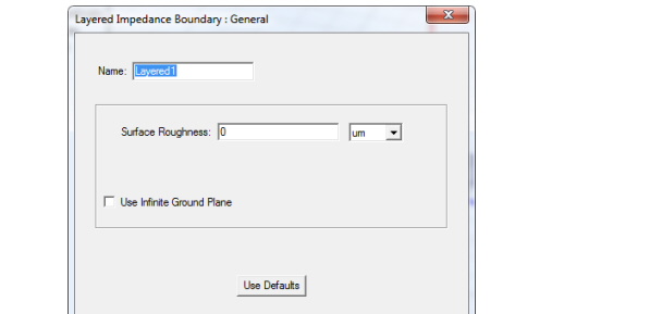
1. Select a surface on which to assign the boundary and click HFSS >Boundaries>Assign>Layered Impedance to bring up the Layered Impedance Boundary dialog box.

2. Enter the Surface Roughness for the layered structure.
If the layered structure is internal to the design, enter the average surface roughness of the two outermost sides. You can assign a variable as this value.
3. Select Infinite Ground Plane if you want the surface to represent an electrically large ground plane when the radiated fields are calculated during post processing.
For designs with layered impedance boundaries, only one infinite ground plane can exist in the design.
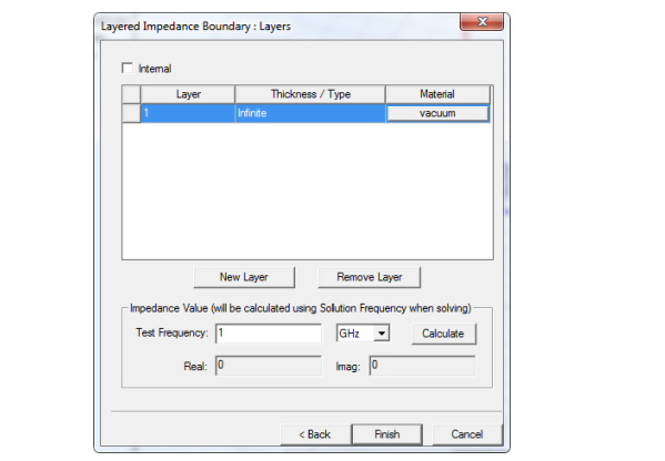
4. Click Next or the Layers tab, depending on the general option setting.

5. If the layered structure is external to the design, do the following:
• By default, HFSS assumes the layered structure is external to the design; the outermost layer of the structure is listed. Select whether this layer is an Infinite, Perfect E, or Perfect H layer from the Thickness/Type list.
If the layered structure is within the 3D model, do the following:
a. Select the Internal option.
b. Enter a thickness for the first layer in the Thickness/Type column. You can assign a variable as this value.
6. To change the first layer’s material, click vacuum and follow the procedure for assigning a material.
7. To add a new layer to the structure:
a. Click New Layer.
The new layer is added at the end of the list.
b. Enter a thickness for the layer in the Thickness/Type column. You can assign a variable as this value.
c. To change the layer’s material, click vacuum and follow the procedure for assigning a material.
8. Optionally, to reorder layers, click the first row square and drag the row to the desired position.
9. Optionally, to view the impedance values that will be calculated based on the data provided, do the following:
a. Enter the frequency at which the solution is being solved in the Test Frequency text box.
b. Click Calculate.
The real and imaginary components of the HFSS-calculated layered impedance value appear.
Note |
A warning will be posted if a fast sweep is defined in a design that contains a layered impedance boundary, since the impedance may only be accurate for the center frequency. |
Related Topics
Technical Notes: Layered Impedance Boundaries
-

国内最全面的HFSS培训课程,包含7套视频教程和2本教材,资深专家讲解,视频操作演示,结合最新工程案例,让HFSS学习不再难...【详细介绍】


