|
微波射频仿真设计 |
|
|
微波射频仿真设计 |
|
| 首页 >> Ansoft Designer >> Ansoft Designer在线帮助文档 |
|
Nexxim Simulator > Voltage-Controlled Voltage Source, Multi-Input Gate
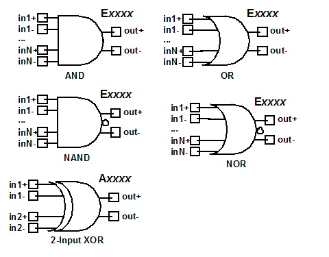 VCVS Gate Netlist FormatThe format for an N-input AND gate VCVS is: Exxxx out+ out- [VCVS] AND(N) in1+ in1- ... inN+ inN- minval1 outval1 ... minvalK outvalK [DELTA=val] [TC1=val] [TC2=val] [SCALE=val] The format for an N-input NAND gate VCVS is: Exxxx out+ out- [VCVS] NAND(N) in1+ in1- ... inN+ inN- minval1 outval1 ... minvalK outvalK [DELTA=val] [TC1=val] [TC2=val] [SCALE=val] The format for an N-input OR gate VCVS is: Exxxx out+ out- [VCVS] OR(N) in1+ in1- ... inN+ inN- minval1 outval1 ... minvalK outvalK [DELTA=val] [TC1=val] [TC2=val] [SCALE=val] The format for an N-input NOR gate VCVS is: Exxxx out+ out- [VCVS] NOR(N) in1+ in1- ... inN+ inN- minval1 outval1 ... minvalK outvalK [DELTA=val] [TC1=val] [TC2=val] [SCALE=val] The format for a 2-input XOR gate VCVS is: Axxxx out+ out- in1+ in1- in2+
in2- [SCALE=val] out+ and out- are the nodes of the voltage output. The entry VCVS is the default for the E element type. in1+ in1- ... inN+ inN- are the positive and negative node pairs for the multiple control voltage inputs. The number of input node pairs (N) in the list must be the same as the value specified for AND(N), NAND(N), OR(N), or NOR(N). The entry component=vcvs_xor is required only for the 2-input VCVS XOR gate. The 2-input VCVS XOR gate syntax uses inputs in1+, in1-, in2+, and in2- and only one parameter, SCALE.
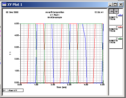
VCVS Gate Netlist ExamplesThese two-input examples assume logic “0” is 0.0 volts output at 0.0 volts input, and logic “1” is 5.0 volts output at 5.0 volts input. Eand2 30 0 VCVS AND(2) 21 0 22 0 Here is a sample simulation showing the output of this element:
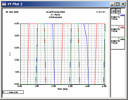
Enand2 40 0 VCVS NAND(2) 23 0 24 0 Here is a sample simulation showing the output of this element:
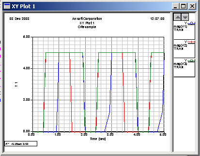
Eor2 50 0 VCVS OR(2) 25 0 26 0 Here is a sample simulation showing the output of this element:
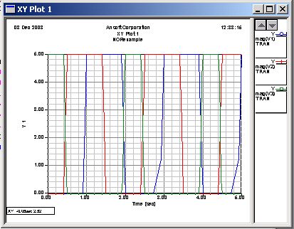
Enor2 60 0 VCVS NOR(2) 27 0 28 0 Here is a sample simulation showing the output of this element:
 NotesThe output for the AND(N), NAND(N), OR(N), and NOR(N)is specified as a function of the inputs using a set of pairs (minval, outval or maxval, outval), separated by spaces and/or commas. Voltages are specified in volts. The pairs should be entered in ascending order of minval or maxval (see Netlist Examples). Any number of pairs may be specified. For AND and NAND gates, the simulator finds the minimum difference between all pairs of inputs: The simulator matches mindiff to the list of entries minval1 ... minvalK in the instance statement, and sets the output to the corresponding outval. When mindiff is equal to the voltage that represents logic “0” or logic “1,” the corresponding output from an AND or NAND gate should be set accordingly. Values of mindiff that are intermediate between the logic “0” and “1” voltages represent transitional values. For intermediate values that are not in the list of minvals, the simulator calculates the corresponding output by interpolation from the given values. The use of the DELTA parameter allows you to control the curvature of the interpolation to guarantee that the 1st derivative of the curve is continuous. For values of mindiff that are below the range of listed input voltages, the simulator sets the output voltage to the one corresponding to the smallest input voltage in the list. For values of mindiff that are above the range of listed input voltages, the simulator sets the output voltage to the one corresponding to the largest input voltage in the list. For OR and NOR gates, the simulator finds the maximum difference between all pairs of inputs: The simulator matches maxdiff to the list of entries maxval1 ... maxvalK in the instance statement, and sets the output to the corresponding outval. When maxdiff is equal to the voltage that represents logic “0” or logic “1,” the corresponding output from an OR or NOR gate should be set accordingly. Values of maxdiff that are intermediate between the logic “0” and “1” voltages represent transitional values. For intermediate values that are not in the list, the simulator calculates the corresponding output by interpolation from the given values, using the DELTA parameter as discussed above. For values of maxdiff that are below the range of listed input voltages, the simulator sets the output voltage to the one corresponding to the smallest input voltage in the list. For values of maxdiff that are above the range of listed input voltages, the simulator sets the output voltage to the one corresponding to the largest input voltage in the list.
HFSS视频教程 ADS视频教程 CST视频教程 Ansoft Designer 中文教程 |
|
Copyright © 2006 - 2013 微波EDA网, All Rights Reserved 业务联系:mweda@163.com |
|


