|
微波射频仿真设计 |
|
|
微波射频仿真设计 |
|
| 首页 >> Ansoft Designer >> Ansoft Designer在线帮助文档 |
|
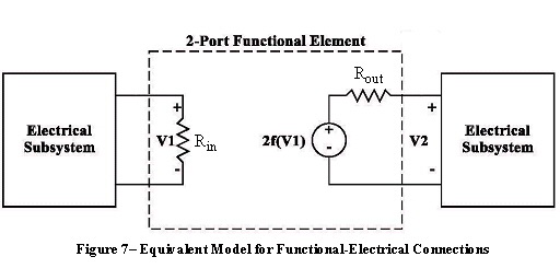
Nexxim Simulator > Assumptions for Nexsys PartitioningThe following assumptions govern the partitioning process. 1. The impedance seen by an electrical component or sub-design looking into an input port of a functional component is assumed to be Rin, always defaulted to an open or infinity Ω (see Figure 7). In other words, when an electrical component or sub-design port is terminated into the input port of a functional component, the termination resistance is Rin. This load resistance can be adjusted by assigning a different value to the Rin parameter of the functional component. This resistance will have no noise contribution.
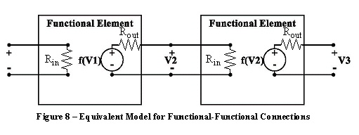
2. The impedance seen by an electrical component or sub-design looking into an output port of a functional component is assumed to be Rout (defaulted to a short or 0Ω) also shown in Figure 7. In other words, when an electrical component or sub-design input port is connected to the output port of a functional component, the assumed source resistance is Rout. This source resistance can be adjusted by assigning a different value to the Rout parameter of the functional component. Note that in reference to Figure 7, the input voltage to the electrical sub-design V2 would equal f(V1) if the impedance seen by the functional component looking into the electrical sub-design is 50Ω, provided that Rout is set to 50Ω. The notation f(.) represents the equivalent signal processing operation of the functional component. 3. The impedance seen by a functional component looking into an input port of another functional component is assumed to be Rin (typically defaulted to infinity) and the impedance seen by a functional component looking into an output port of another functional component is assumed to be Rout (typically defaulted to zero). This is illustrated in Figure 8 below.
4. All nonlinear electrical two-port components (AMP and MIXER) are assumed to be unidirectional (i.e., S12 = 0). Each nonlinear electrical component is partitioned into three segments: a linear active input stage, a nonlinear functional stage, and a linear electrical passive output stage. This arrangement will be discussed later in more detail. 5. During signal analysis, any signal path in the system is described by its complex envelope and carrier frequency (i.e., the triplet (I(t), Q(t), fc)) as well as the simulation time step ts. In general, the signal ((I(t), Q(t)) information bandwidth, carrier frequency fc, and simulation time step ts vary from one point in the system to another. The user must measure the signal ((I(t), Q(t)) information bandwidth, the carrier frequency fc, and simulation time step ts at the correct points in the system to generate meaningful results. A baseband signal is described by its real signal value and the time step. 6. If Nexxim sources are interfaced with Nexsys components, a SAMPLER component must be placed at the physical/functional interface, otherwise the simulation engine will issue an error. The user specifies the sampling rate for the SAMPLER component. 7. An ENVELOPEADAPTOR component must be placed at the interface of bandpass signal (or modulated signal) entering a Nexxim sub-circuit from a Nexsys functional component. The ENVELOPEADAPTOR component helps the simulation engine to recognize what circuit simulation analysis is needed to call to solve the Nexxim sub-circuit.
HFSS视频教程 ADS视频教程 CST视频教程 Ansoft Designer 中文教程 |
|
Copyright © 2006 - 2013 微波EDA网, All Rights Reserved 业务联系:mweda@163.com |
|