|
微波射频仿真设计 |
|
|
微波射频仿真设计 |
|
| 首页 >> Ansoft Designer >> Ansoft Designer在线帮助文档 |
|
Using Component Libraries > The Edit Padstack Definition DialogThe Edit Padstack Definition dialog controls padstack property values. You can access the dialog by Creating a New Padstack or Editing an Existing Padstack.
The following controls are available in the Edit Padstack Definition dialog. Depending upon the context and padstack being edited, at times only a subset of the following options may appear.
General • Name — Specifies the name of the padstack. • Via Material — Specifies the material for plating the via/pin hole, and the associated button directly below the checkbox displays the material name. Clicking the button opens the Materials tab in the Select Definitions dialog so that a new material can be chosen. The default via material is copper. • Plating Percent — The thickness of the material plating in the hole.
Hole • Shape — Choices are None, Circle, Square, Rectangle and Polygon. As with pads, the Polygons choice supports imported padstacks with holes. • Diameter — Specifies the size of the hole. • Range can specify the hole range to be: o Through all of the layout stackup layers o Beginning at the upper pad of the padstack and continuing to the lowest elevation of the layout stackup layers o Beginning at the highest elevation of the layout stackup layers and ending at the lowest pad of the padstack o Beginning at the upper pad and ending at the lowest pad of the padstack
Solderball • Shape — Specifies the shape of the solderball; choices are none, cylinder, and spheroid. • Diameter — Specifies the diameter of the solderball. • Mid diameter — Specifies the mid diameter of the solderball. • Solder — Click this button to open the Material Editor for the solderball in order to specify the material used. • Connection — Select to specify the location of the solderball either above or below the padstack hole.
Layers • None of the Layers section grid control cells are directly editable. • When one or more rows in the Layers section are selected, controls are enabled and can be used to change the pad settings for selected rows. • Add layer inserts a new layer above the selected row. • Remove layer removes the selected row(s). You may also rearrange rows to be any order.
Layer Settings The Layer settings section displays the pad settings for the padstack definition layers. • Pad and Anti pad shape choices are None, Circle, Square, Rectangle, Oval, Bullet, and Polygon. • Thermal pad shape choices are None, Round45, Round90, Square45, Square90, and Polygon. • Connection pt allows you to choose a direction in degrees or specify None.
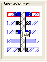
Cross Section view Displays all the definition layers and their pads from a side view. The selected layers are highlighted. Tool tips indicating layer/hole/plating/pad appear when the mouse hovers over one of these shapes. 
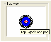
Top View Displays the pads of the selected layers from a top down perspective. Tool tips indicating hole/plating/pad on a layer appear when the mouse hovers over one of these shapes. 
HFSS视频教程 ADS视频教程 CST视频教程 Ansoft Designer 中文教程 |
|
Copyright © 2006 - 2013 微波EDA网, All Rights Reserved 业务联系:mweda@163.com |
|