|
微波射频仿真设计 |
|
|
微波射频仿真设计 |
|
| 首页 >> Ansoft Designer >> Ansoft Designer在线帮助文档 |
|
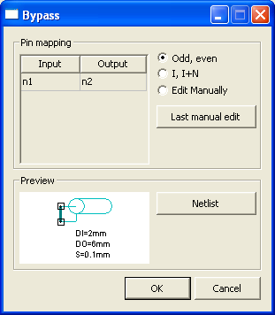
Dynamic Links and Solver On Demand > BypassIn the Solver on Demand tab of the Edit Component dialog, when you choose Bypass from the model pulldown menu and click Add, the following bypass definition dialog appears. Alertnately, If a Bypass model is already listed in the Edit Component dialog, click on its Define Model column button to open the following dialog.

The Bypass Solver-on-Demand model allows you to auto-generate netlists to bypass a component through .connect expressions. Using the Bypass definition dialog, you can customize the pin connections of a component. (For two-port components, a Bypass model is created automatically. For components with more than two ports, it is necessary to define the Bypass pin mapping.) • The Bypass definition dialog displays the current pin mappings. • Select Odd, even or I, I+N to use a pre-defined pin combination. • Select the Edit radio button to manually define connections. To define a connection, in the pin mapping grid, first select from the Input pulldown list, then select from the Output pulldown list. • Select Last manual edit to cancel any changes you have made and return to the last saved pin combination. • Select Reset to reset the pin combinations to their preset defaults. • Click Netlist to see the Bypass netlist. • Once the pin combination is defined, a preview of the component's design is displayed in the Preview window.
Click OK to save your changes and close the dialog, or click Cancel to close the dialog without saving any changes. HFSS视频教程 ADS视频教程 CST视频教程 Ansoft Designer 中文教程 |
|
Copyright © 2006 - 2013 微波EDA网, All Rights Reserved 业务联系:mweda@163.com |
|