|
Port Mode View
From the ,
select the port mode and component you want to visualize. The entries
in the navigation tree depend on the properties of the ports.
General naming conventions of folder entries
|

|
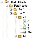
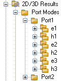
For every waveguide
port you can visualize the electric and magnetic fields as 2D vector plots
by clicking on the folder named eM (electric) and hM (magnetic), respectively.
M denotes the number
of the mode of the waveguide port. The picture on the left shows the folder
entries for the electric and magnetic fields of port 2 for the first and
second mode. |
|
|
In addition, you can
visualize components of the fields and the magnitude of the fields in
a 2D scalar plot.
Click on the X,Y or
Z entry to visualize the respective field component. To visualize the
magnitude of the field, click on the Abs entry. |
Inhomogeneous waveguide ports
|
|
Frequency
Domain Solver: If the modelled structure contains inhomogeneous
waveguide ports, the electromagnetic fields of the mode are calculated
at several frequency samples (for detailed information, see the Waveguide
Port Overview page).
Time
Domain Solver: If the modelled structure contains inhomogeneous
waveguide ports, and if either the full deembedding feature or the broadband
port is activated, the electromagnetic fields of the mode are calculated
at several frequency samples (for detailed information see the Waveguide
Port Overview page).
To distinguish the
fields at the different frequency samples, select the appropriate folder
and activate the main view with a mouse click. Now use the page
up and page
down keys to change
the frequency of the mode. |
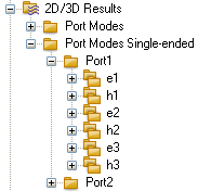
Single-ended port modes
|
|
For single-ended ports
the corresponding modes can be accessed via an additional folder showing
the single-ended modes. They correspond to the single-ended pin description. |
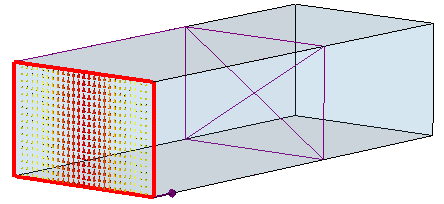
Evanescent port modes
|
|
In the case of evanescent
modes in addition to the port mode, the distance where the mode is damped
to -40 dB is displayed, as demonstrated in the picture.
|
In the lower left corner the following values
are plotted:
Type: E-Field or H-Field Maximum: In the case of a vector plot,
the value of the maximum arrow. Component: In the case of a scalar plot,
this parameter determines which component is plotted. Mode type: The type of the plotted mode:
TEM, Quasi TEM, TE, TM or Unknown Accuracy: The accuracy of the calculation
for the plotted mode. Fcutoff: In the case of a TE or TM mode,
this is the cutoff frequency. Beta: The mode’s Beta value. Alpha: In the case of an unknown mode
type or TE / TM mode,this is the Alpha value. Dist.-40 dB: The distance where
the field values of an evanescent mode are damped to -40 dB. Wave Imp.: The wave impedance in Ohms.
See Waveguide
Port Overview for impedance definitions. Line Imp.: For mode type TEM or Quasi
TEM, this is the line impedance in Ohms. See Waveguide
Port Overview for impedance definitions. In case of a complex line
impedance, its magnitude is displayed. Imp. ZPV re/im: This is the impedance
in Ohms which is determined by the computed voltage
along a line and the mode's complex power. re
and im indicate its real and
imaginary part. See Waveguide
Port Overview for impedance definitions. Plane at x/y/z: Coordinate of the port
plane in the specific orientation (x/y/z). Frequency: The frequency for which the
modes and their parameters have been calculated. This is the center of
the frequency range given in Frequency
Range Settings. Phase: The phase for which the mode
is plotted. Maximum-2d: Displays the value and location
of the maximum field, depending on the selected type.
See also
Waveguide
Port Overview, Post
Processing Overview


HFSS视频教程
ADS视频教程
CST视频教程
Ansoft Designer 中文教程
|
|
