![]()
![]()
|
Transient Solver: |
|
|
Frequency Domain Solver Tetrahedral: |
|
Introduction and Model Dimensions
Results of the Frequency Domain Solver
Comparison of the Solver Results
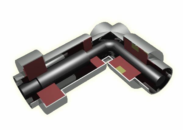
In this tutorial you learn how to simulate coaxial structures. As a typical example for a coaxial structure you will analyze a 90 degree coaxial connector. The following explanations on how to model and analyze this device can also be applied to other devices containing coaxial components.
CST MICROWAVE STUDIO provides a wide variety of different solvers and results. This tutorial, however, concentrates on S-Parameters. The results will be obtained by two alternative techniques. One simulation will be performed in time domain on a hexahedral mesh and the other in frequency domain on a tetrahedral mesh.
We strongly suggest that you carefully read through the CST STUDIO SUITE Getting Started and CST MICROWAVE STUDIO Workflow and Solver Overview manual before starting this tutorial.
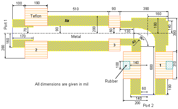
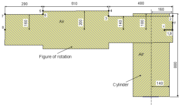
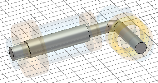
The structure shown above consists of several coaxial sections. The inner conductor of the connector is made from perfect electrically conducting material and is embedded in vacuum. This structure is mounted at three locations with Teflon rings. One of these fixtures additionally contains a rubber ring.
This tutorial will take you step-by-step through the construction of your model, and relevant screen shots will be provided so that you can double-check your entries along the way.
o Create a New Project
After launching the CST STUDIO SUITE
you will enter the start screen showing you a list of recently opened
projects and allowing you to specify the application which suits your
requirements best. The easiest way to get started is to configure a project
template which defines the basic settings that are meaningful for your
typical application. Therefore click on the Create
Project button ![]() in the New Project section.
in the New Project section.
Next you should choose the application area, which is Microwaves & RF for the example in this tutorial and then select the workflow by double-clicking on the corresponding entry.
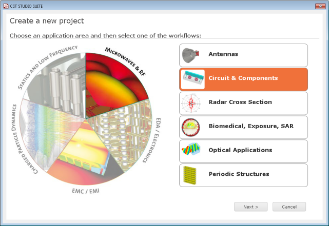
For the Coaxial structure, please select
Circuits & Components ![]() Coaxial
(TEM) Connectors
Coaxial
(TEM) Connectors ![]() Time Domain Solver
Time Domain Solver ![]() .
.
At last you are requested to select the units which fit your application best. For the Coaxial structure, please select the dimensions as follows:
|
Dimensions: |
mil |
|
Frequency: |
GHz |
|
Time: |
ns |
For the specific application in this tutorial the other settings can be left unchanged. After clicking the Next button, you can give the project template a name and review a summary of your initial settings:
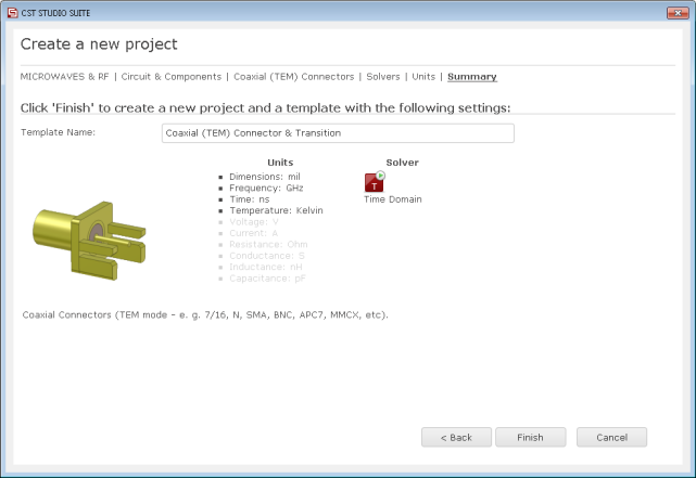
Finally click the Finish button to save the project template and to create a new project with appropriate settings. CST MICROWAVE STUDIO will be launched automatically due to the choice of the application area Microwaves & RF.
Please note: When you click again on the File: New and Recent you will see that the recently defined template appears below the Project Templates section. For further projects in the same application area you can simply click on this template entry to launch CST MICROWAVE STUDIO with useful basic settings. It is not necessary to define a new template each time. You are now able to start the software with reasonable initial settings quickly with just one click on the corresponding template.
Please
note: All settings made for a project template can be modified
later on during the construction of your model. For example, the units
can be modified in the units dialog box (Home:Settings ![]() Units
Units ![]() ) and the solver type can be selected
in the Home:Simulation
) and the solver type can be selected
in the Home:Simulation ![]() Start Simulation drop-down
list.
Start Simulation drop-down
list.
o Set the Working Planes Properties
The next step is usually to set the
working plane properties in order to make the drawing plane large enough
for your device. Since the structure has a maximum extent of 1320
mil along a coordinate direction, the working plane size should be set
to at least 1500 mil. These settings can be changed in the dialog
box that opens after selecting View:Visibility
![]() Working Plane
Working Plane ![]()
![]() Working Plane Properties.
Working Plane Properties.
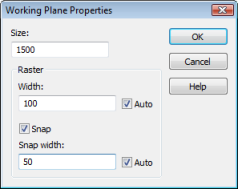
In this dialog box, you should set the Size to 1500 (the unit which has previously been set to mil is displayed in the status bar), the Raster width to 100 and the Snap width to 50 to obtain a reasonably spaced grid. Please confirm these settings by pressing the OK button.
o Draw the Air Parts
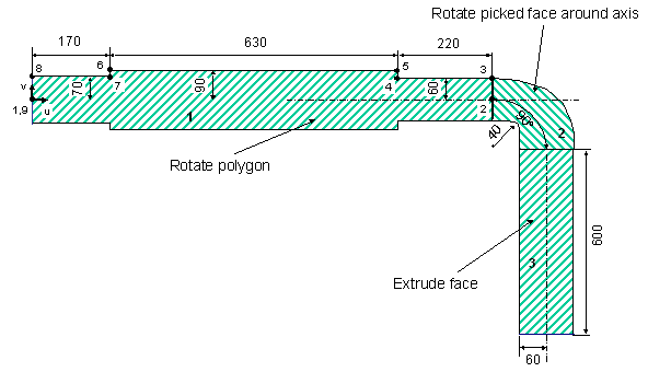
In this structure, the air can be easily modeled by uniting two rotational symmetric parts (a figure of rotation and a cylinder) as shown in the following diagram:
In the first step, you can begin drawing
the figure of rotation. Because the cross section profile is a simple
polygon, you do not need to use the curve modeling tools here (please
refer to the CST STUDIO
SUITE Getting
Started manual for more information on this advanced
functionality). For polygonal cross sections it is more convenient to
use the figure of rotation tool, activated by selecting Modeling: Shapes ![]() Extrusions
Extrusions ![]() Rotate
Rotate ![]() .
.
Since no face has been previously picked, the tool will automatically enter a polygon definition mode and request that you enter the polygons points. You can do this by either double-clicking on each points coordinates on the drawing plane or entering the values numerically. Since the latter approach may be more convenient, we suggest pressing the Tab key and entering the coordinates in the dialog box. All polygon points can thus be entered step-by-step according to the following table. Whenever you make a mistake, you can delete the most recently entered point by pressing the Backspace key. Arbitrary changes can also be made at the end of the input process.
|
Point |
X |
Y |
|
1 |
0 |
0 |
|
2 |
0 |
140 |
|
3 |
480 |
140 |
|
4 |
480 |
200 |
|
5 |
990 |
200 |
|
6 |
990 |
160 |
|
7 |
1280 |
160 |
|
8 |
1280 |
0 |
|
9 |
0 |
0 |
After the last point has been entered, the polygon will then be closed. The Rotate Profile dialog box will then automatically appear.
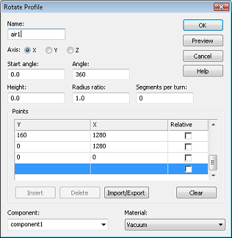
This dialog box allows you to review the coordinate settings in the list. If you encounter any mistakes, you can easily change the values by double-clicking on the incorrect coordinate entry field.
The next step is to assign a specific Component and a Material to the shape. In this case, the default settings with component1 and Vacuum are practically appropriate.
Please note: The use of different components allows you to collect several solids into specific groups, independent of their material behavior. However, here it is convenient to construct the complete connector as a representation of one component.
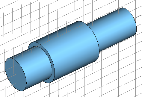
Finally, assign a proper Name (e.g. air1) to the shape and press the OK button to finish the creation of the solid. The picture below shows how your structure should appear:
Construction of the second air part
by creating a cylinder can be simplified if a local or rather working
coordinate system (WCS) is introduced first. You can activate the
working coordinate system by selecting Modeling:
WCS ![]() Local
WCS
Local
WCS ![]() . Afterwards, the origin of this coordinate
system should be moved by selecting Modeling:
WCS
. Afterwards, the origin of this coordinate
system should be moved by selecting Modeling:
WCS ![]() Transform
WCS
Transform
WCS ![]() . The following dialog box allows you
to enter a vector along which the origin of the working coordinate system
will be moved.
. The following dialog box allows you
to enter a vector along which the origin of the working coordinate system
will be moved.
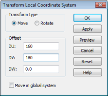
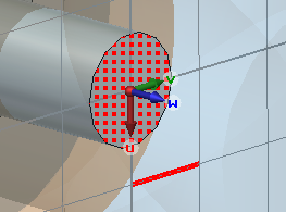
You should shift the origin by 160 mil
along the u direction and by 180 mil along the v direction in order to
position the WCS at the center of the cylinders base. Afterwards,
rotate the WCS along its u-axis by 90 degrees. Therefore select Modeling:
WCS ![]() Transform
WCS
Transform
WCS ![]() and
define Rotate +90ТА around U axis or using the shortcut Shift+U. The
model should then look as follows:
and
define Rotate +90ТА around U axis or using the shortcut Shift+U. The
model should then look as follows:
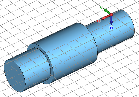
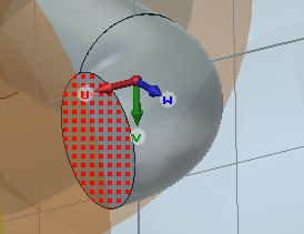
The second air part can now be created
using the cylinder tool: Modeling:
Shapes
![]() Cylinder
Cylinder ![]() .
Once the cylinder creation mode is active, you are requested to pick the
center of the cylinder. Because this is now the origin of the working
coordinate system, you can simply press Shift+Tab to open the dialog
box for numerically entering the coordinates and confirm the settings
by pressing OK (please note that holding down the Shift
key while pressing the Tab key opens the dialog box with the coordinate
values initially set to zero rather than the current mouse pointers location).
.
Once the cylinder creation mode is active, you are requested to pick the
center of the cylinder. Because this is now the origin of the working
coordinate system, you can simply press Shift+Tab to open the dialog
box for numerically entering the coordinates and confirm the settings
by pressing OK (please note that holding down the Shift
key while pressing the Tab key opens the dialog box with the coordinate
values initially set to zero rather than the current mouse pointers location).
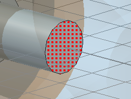
You are now requested to enter the outer radius of the cylinder. Please press the Tab key again and set the Radius to 140 before pressing the OK button. The Height of the cylinder can then be set to 880 in the same manner. Skip the definition of the inner radius by pressing the Esc key (the air should be modeled as solid cylinder here) and check your settings in the following dialog box:
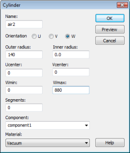
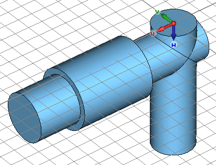
Finally, set the Name of the cylinder to air2 and verify that the solid again is associated with the vacuum Material. Confirm your settings by pressing OK. Since the two air parts overlap each other, the shape intersection dialog box will open automatically, asking you to select a Boolean operation to combine the shapes. Please select the operation Add both shapes to unite both parts and press the OK button. Your model should then finally look as follows:
o Model the Teflon and Rubber Cylinders
After successfully modeling the air
parts, you can now create the first Teflon cylinder. Again it is
advantageous to move the WCS to the middle of the Teflon cylinder by selecting
Modeling:
WCS
![]() Transform WCS
Transform WCS ![]() and enter the expression 390 + 310 / 2 in the DW field to move
the WCS along the w-axis by this amount. Please refer to the structures
schematic drawing earlier in this tutorial to confirm that the new origin
of the WCS is located in the center of the first Teflon cylinder.
and enter the expression 390 + 310 / 2 in the DW field to move
the WCS along the w-axis by this amount. Please refer to the structures
schematic drawing earlier in this tutorial to confirm that the new origin
of the WCS is located in the center of the first Teflon cylinder.
Once the coordinate system is properly
located, you can now easily model the Teflon cylinder by selecting Modeling:
Shapes
![]() Cylinder
Cylinder ![]() .
When you are requested to enter the cylinders center, press Shift+Tab
and check the coordinate values U=0, V=0 before clicking the OK
button.
.
When you are requested to enter the cylinders center, press Shift+Tab
and check the coordinate values U=0, V=0 before clicking the OK
button.
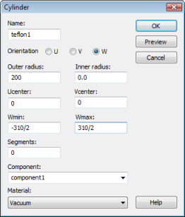
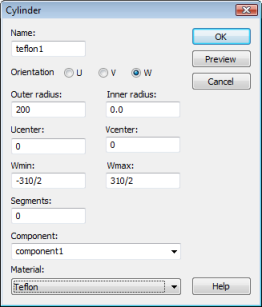
Afterwards, press the Tab key again to set the cylinders outer radius to 200. The height of the cylinder should then be set to 310 / 2 (you are currently modeling only one half of the cylinder) in the same way. After skipping the definition of the inner radius by pressing the Esc key, the cylinder creation dialog box should appear, where you should assign a proper Name (e.g. teflon1) to the shape before you also enter the expression "-310 / 2" in the Wmin field to properly set the cylinders full length:
You can skip the Component setting because the complete connector will be constructed as one component. However, the cylinders material is currently set to Vacuum. In order to change this, select [New material...] in the Material dropdown list, opening the material parameter dialog box:
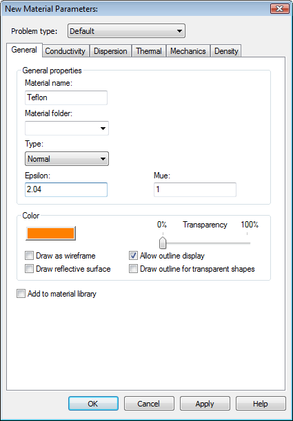
In this dialog box you should set the Material name to Teflon and the Type to be a Normal dielectric material. Afterwards, you can specify the dielectric constant of Teflon by entering 2.04 in the Epsilon field. Select the Change button in the Color frame and choose a color.
Finally, you should check your settings in the dialog box again before pressing the OK button to store the materials parameters.
Please note: The defined material Teflon will now be available inside the current project for the further creation of other solids. However, if you also want to save this specific material definition for other projects, you may check the button Add to material library. You will have access to this material database by clicking on Load from Material Library in the Materials context menu in the navigation tree.
The dialog for the cylinder creation should now look as follows:
After checking the current settings, create the cylinder by pressing the OK button. Since the Teflon cylinder overlaps the previously modeled air parts, the shape intersection dialog box will appear again:
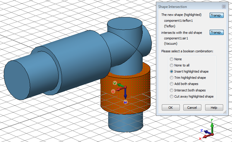
Here, you should choose to insert the new Teflon cylinder into the air part by selecting Insert highlighted shape before pressing the OK button. Please refer to the CST STUDIO SUITE Getting Started manual for more information on Boolean operations.
Afterwards, the rubber ring inside the first Teflon cylinder can be modeled analogously:
1.
Activate the cylinder creation tool (Modeling:
Shapes
![]() Cylinder
Cylinder ![]() ).
).
2. Press Shift+Tab and set the center point to U = 0, V = 0.
3. Press Tab and set the Radius to 200.
4. Press Tab and set the Height to 100/2.
5. Press Tab and set the inner Radius to 140.
6. Set the Name to rubber and enter -100/2 in the Wmin field.
7. Select [New Material...] from the Material dropdown list to create a new material.
8. In the material properties dialog box set the Material name to Rubber, its Type to Normal and its dielectric constant Epsilon to 2.75.
9. Choose a color by pressing the Change button and confirm the material creation by pressing OK.
10. Back in the cylinder creation dialog box, verify the material assignment to Rubber and press the OK button.
11. In the shape intersection dialog box, choose Insert highlighted shape and press OK.
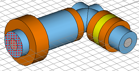
After successfully performing all above steps, your model should look as follows:
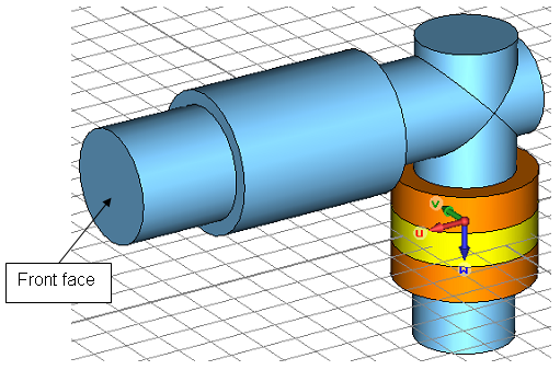
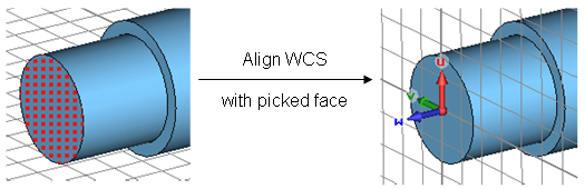
Before you continue with the construction of the two remaining Teflon rings, the working coordinate system should be aligned with the front face shown in the picture above.
Therefore, please activate the pick
face tool by either selecting Modeling: Picks ![]() Picks
Picks ![]()
![]() Pick
Point, Edge or Face (S) or just using the shortcut f (while the main view is
active). Afterwards, the front face should be selected by double-clicking
on it. The working coordinate system is aligned with the front face
by selecting Modeling:
WCS
Pick
Point, Edge or Face (S) or just using the shortcut f (while the main view is
active). Afterwards, the front face should be selected by double-clicking
on it. The working coordinate system is aligned with the front face
by selecting Modeling:
WCS ![]() Align WCS
Align WCS ![]() or using shortcut w:
or using shortcut w:
The next step is to move the WCS to
the location of the second Teflon cylinders base. Therefore, please
select again Modeling:
WCS ![]() Transform
WCS
Transform
WCS ![]() and enter "-290" in the DW field
before pressing OK. Now you can straightforwardly model the
second Teflon cylinder as shown in the structures drawing.
and enter "-290" in the DW field
before pressing OK. Now you can straightforwardly model the
second Teflon cylinder as shown in the structures drawing.
1.
Activate the cylinder creation tool (Modeling:
Shapes
![]() Cylinder
Cylinder ![]() ).
).
2. Press Shift+Tab and set the center point to U = 0, V = 0.
3. Press Tab and set the Radius to 280.
4. Press Tab and set the Height to 190.
5. Press Tab and set the inner Radius to 90.
6. In the cylinder creation dialog box set the Name to teflon2 and select the previously defined Material Teflon before pressing OK.
7. In the shape intersection dialog box, choose Insert highlighted shape and press OK.
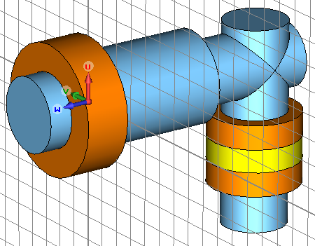
The model should then look as follows:
For the creation of the third Teflon ring you should again move the WCS to the proper location:
1.
Select Modeling:
WCS ![]() Transform
WCS
Transform
WCS ![]() to open the move WCS dialog box.
to open the move WCS dialog box.
2. Enter -600 in the DW field and press OK.
The construction of the Teflon ring can then be performed by:
1.
Activate the cylinder creation tool (Modeling:
Shapes
![]() Cylinder
Cylinder ![]() ).
).
2. Press Shift+Tab and set the center point to U = 0, V = 0.
3. Press Tab and set the Radius to 200.
4. Press Tab and set the Height to 90.
5. Press Esc to skip the definition of the inner radius.
6. In the cylinder creation dialog box, set the Name to teflon3 and select the previously defined Material Teflon before pressing OK.
7. In the shape intersection dialog box, choose Insert highlighted shape and press OK.
After successfully completing these steps, the model should look as follows:
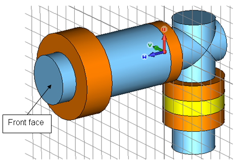
o Model the Inner Conductor
Creation of the inner conductor of the coaxial cable can again be simplified by aligning the working coordinate system with the front face shown in the above picture:
1.
Activate the pick face tool (Modeling:
Picks![]() Picks
Picks ![]()
![]() Pick Point, Edge or Face (S) )
Pick Point, Edge or Face (S) )
2. Double-click on the front face shown above.
3.
Align the WCS with the picked face (Modeling:
WCS ![]() Align WCS
Align WCS ![]() )
)
The new location of the working coordinate system should then be shown as pictured below:
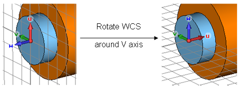
Next, the WCS should be rotated such
that its u axis points into the structure by invoking the command Modeling:
WCS ![]() Transform
WCS
Transform
WCS ![]() and define Rotate +90ТА around
V axis (Shift+v).
and define Rotate +90ТА around
V axis (Shift+v).
Now the first part of the inner conductor can be modeled by a figure of rotation that is shown in the schematic drawing below:
Since the construction of a figure of rotation has already been explained in detail earlier in this tutorial, we will only give a short list of steps:
1.
Activate the wire frame visualization mode by
pressing View: Visibility ![]() Wire Frame
Wire Frame ![]() or using the shortcut Ctrl+w. This
will allow you to follow the construction; otherwise, the parts of the
inner conductor will be hidden inside the previously created shapes.
or using the shortcut Ctrl+w. This
will allow you to follow the construction; otherwise, the parts of the
inner conductor will be hidden inside the previously created shapes.
2.
Activate the figure of rotation tool (Modeling: Shapes ![]() Extrusions
Extrusions
![]() Rotate
Rotate ![]() .)
.)
3. Enter the points shown in the table below by pressing the Tab key and specifying the coordinate values numerically:
|
Point |
U |
V |
|
1 |
0 |
0 |
|
2 |
1020 |
0 |
|
3 |
1020 |
60 |
|
4 |
800 |
60 |
|
5 |
800 |
90 |
|
6 |
170 |
90 |
|
7 |
170 |
70 |
|
8 |
0 |
70 |
|
9 |
0 |
0 |
4. Once the last point has been defined the polygon is closed. The rotate profile creation dialog box will open. In this dialog box check the points coordinates, set the Name of the shape to conductor1 and change the Material assignment to PEC before pressing OK.
After successfully performing these steps, the structure should look as follows:
Please select the inner conductor by
either double-clicking on it in the view or by selecting component1
![]() conductor1
from the navigation tree. Once this is done, you may deactivate
the wire frame plot mode (View: Visibility
conductor1
from the navigation tree. Once this is done, you may deactivate
the wire frame plot mode (View: Visibility ![]() Wire Frame
Wire Frame ![]() or Ctrl+w):
or Ctrl+w):

The next step is to align the working
coordinate system with the inner conductors end face shown above.
Therefore, rotate the view to ensure that the end face is visible (select
View: Mouse Control ![]() Rotate
Rotate ![]() and drag the mouse while pressing
the left button). Afterwards, activate the general pick tools (Modeling:
Picks
and drag the mouse while pressing
the left button). Afterwards, activate the general pick tools (Modeling:
Picks ![]() Picks
Picks ![]()
![]() Pick Point, Edge or Face
(S)) and double-click on the desired face.
Pick Point, Edge or Face
(S)) and double-click on the desired face.
Now, align the WCS with this face by
pressing Modeling:
WCS ![]() Align WCS
Align WCS ![]() or shortcut w.
The next step is to define a rotation axis by selecting Modeling:
Picks
or shortcut w.
The next step is to define a rotation axis by selecting Modeling:
Picks ![]() Picks
Picks ![]() Edge from
Coordinates
Edge from
Coordinates ![]() . Enter the first points coordinates
by pressing the Tab key (U = 100, V = 0)
and the coordinates of the second point (U = 100, V = 100)
in the same manner. Finally, check and confirm the settings in the
dialog box.
. Enter the first points coordinates
by pressing the Tab key (U = 100, V = 0)
and the coordinates of the second point (U = 100, V = 100)
in the same manner. Finally, check and confirm the settings in the
dialog box.
Afterwards you need to select the previously
picked face once again (Modeling:
Picks ![]() Picks
Picks ![]()
![]() Pick Point,
Edge or Face (S) + double-click on
the face). Activate the rotate face mode by selecting Modeling:
Shapes
Pick Point,
Edge or Face (S) + double-click on
the face). Activate the rotate face mode by selecting Modeling:
Shapes ![]() Extrusions
Extrusions ![]() Rotate
Rotate
![]() . Because a face has been previously picked,
the definition of polygon points is skipped and a dialog box is opened
immediately:
. Because a face has been previously picked,
the definition of polygon points is skipped and a dialog box is opened
immediately:

In this dialog box, you should first assign a proper Name (e.g. conductor2) to the shape. Because the rotation axis is aligned with the negative v-axis direction and the rotation angle is specified in a right-handed system, the Angle must be set to 90 degrees (the rotation axis is visualized by a blue arrow while the dialog box is open). If not already set, change the Material assignment to PEC and press the OK button.
The last step in the models geometric construction process is to create the third conductor by extruding the end face of the figure of rotation defined above. Rotate the view to obtain a picture similar to the following:
Afterwards, select conductor2 and pick
the end face of the conductor as shown in the above picture (Modeling:
Picks ![]() Picks
Picks ![]()
![]() Pick Point,
Edge or Face (S) +double-click on the end
face).
Pick Point,
Edge or Face (S) +double-click on the end
face).
You can now open the Extrude Face dialog
box by selecting Modeling:
Shapes ![]() Extrude
Extrude ![]() . As with the figure of rotation, a polygon definition
mode will be entered by the extrude tool if no face has been previously
selected.
. As with the figure of rotation, a polygon definition
mode will be entered by the extrude tool if no face has been previously
selected.
In this dialog box, please assign a proper Name (e.g. conductor3), set the Height to 600 (mil) and the Material assignment to PEC before pressing the OK button. Your structure should then look as follows:
To this point, only the structure itself has been modeled. Now it is necessary to define some solver-specific elements. For an S-parameter calculation, you need to define input and output ports. Additionally, the simulation needs to know how the calculation domain should be terminated at its bounds.
o Define Ports
Each port that is defined will simulate an infinitely long waveguide (here a coaxial cable) that is connected to the structure at the ports plane. Waveguide ports are the most accurate way to calculate the S-Parameters of filters and should therefore be used in this case.
Since a waveguide port is based on the two dimensional mode patterns in the waveguides cross-section, the port must be defined large enough to entirely cover these mode fields. In the case of a coaxial cable, the port has to completely cover the coaxial cables substrate.
Before you continue with the port definition, please clear the selection by either double-clicking on the views background or selecting Components in the navigation tree.
The ports extent can be defined either
numerically or, as is more convenient here, by picking the face to be
covered by the port. Therefore, activate the general pick tool (Modeling:
Picks ![]() Picks
Picks ![]()
![]() Pick Point,
Edge or Face (S)) and double-click the substrates
port face at the first port as shown in the picture below:
Pick Point,
Edge or Face (S)) and double-click the substrates
port face at the first port as shown in the picture below:
Please open the waveguide dialog box
(Simulation:
Sources and Loads ![]() Waveguide
Port
Waveguide
Port ![]() ) to define the first
port 1:
) to define the first
port 1:
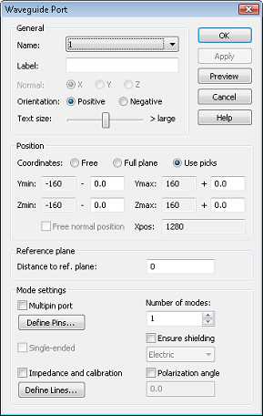
Whenever a face is picked before the port dialog is opened, the ports location and size will automatically be defined by the picked faces extent. Thus the ports Position (transversal as well as normal) is initially set to Use picks. You can accept this setting. The next step is to choose how many modes should be considered by the port. For coaxial devices, we usually have only a single propagating mode. Therefore, you should simply keep the default of one mode.
Finally, check the settings in the dialog box and press the OK button to create the port:
Now you can repeat the same steps for the definition of the second port:
1.
Pick the corresponding substrates port face (Modeling:
Picks ![]() Picks
Picks ![]()
![]() Pick Point,
Edge or Face (S)).
Pick Point,
Edge or Face (S)).
2.
Open the waveguide dialog box (Simulation:
Sources and Loads ![]() Waveguide
Port
Waveguide
Port ![]() .)
.)
3. Press OK to store the ports settings.
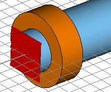
Your model including the ports should now look as follows:

o Define Boundary Conditions and Symmetries
Before you start the solver, you should
always check the boundary and symmetry conditions. This is most
easily accomplished by entering the boundary definition mode by selecting
Simulation:
Settings ![]() Boundaries
Boundaries ![]() . The boundary conditions will then become visualized
in the main view as follows:
. The boundary conditions will then become visualized
in the main view as follows:
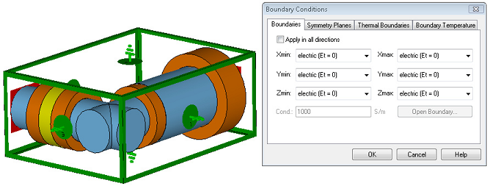
Here, all boundary conditions are set to electric which means that the structure is embedded in a perfect electrically conducting housing. These defaults are appropriate for this example.
Due to the structures symmetry to the XY plane and the fact that the magnetic field in the coaxial cable is perpendicular to this plane, a symmetry condition can be used. This symmetry reduces the time required for the simulation by a factor of two.
Please enter the symmetry plane definition mode by activating the Symmetry Planes tab in the dialog box. By setting the symmetry plane XY to magnetic, you force the solver to calculate only the modes that have no tangential magnetic field component on these planes (thereby forcing the electric field to be tangential to these planes).The screen should then look as follows:
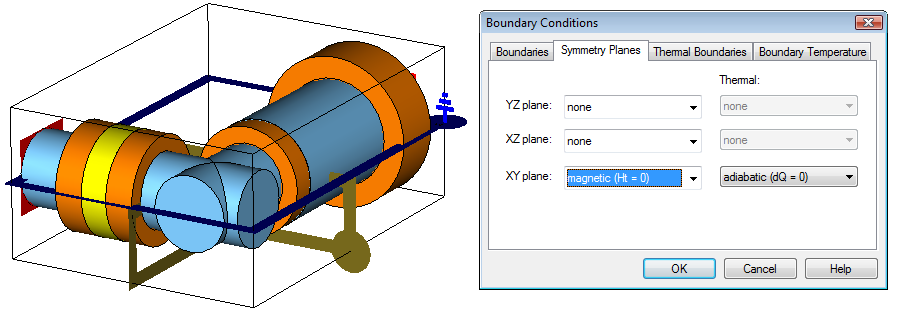
Please note that you also could double-click on the symmetry planes handle and choose the proper symmetry condition from the context menu.
Finally, press the OK button to complete this step.
In general, you should always make use of symmetry conditions whenever possible to reduce calculation times by a factor of two to eight.
o Define the Frequency Range
The frequency range for the simulation should be chosen with care. Different considerations must be made when using a transient solver or a frequency domain solver (see next chapter for details).
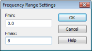
For this example, we will choose a frequency
range from 0 to 8 GHz. Open the frequency range dialog box Simulation: Settings ![]() Frequency
Frequency
![]() and enter the range of 0 to 8 (GHz) before pressing the OK button
(the frequency unit has previously been set to GHz and is displayed in
the status bar):
and enter the range of 0 to 8 (GHz) before pressing the OK button
(the frequency unit has previously been set to GHz and is displayed in
the status bar):
o Define Field Monitors
CST MICROWAVE STUDIO uses the concept of monitors to specify which field data to store. In addition to choosing the type, you can also specify whether the field is recorded at a fixed frequency or at a sequence of time samples (the latter case applies only to the transient solver). You may define as many monitors as necessary to obtain the fields at various frequencies. For the transient solver, all monitors are calculated from a single simulation run by the Fourier Transform. Consequently, the computational overhead for a defined monitor is relatively small.
Please note that an excessive number of field monitors may significantly increase the memory space required for the simulation.
Assume that you are interested in the
current distribution on the coaxial cables conductors at several frequencies
(2, 4, 6 and 8 GHz). To add field monitors, select Simulation:
Monitors ![]() Field Monitor
Field Monitor ![]() .
.
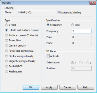
In this dialog box, you should first select the Type H-Field / Surface current before specifying the frequency for the monitor in the Frequency field. Afterwards, press the Apply button to store the monitors data. Please define monitors for the following frequencies: 2, 4, 6, 8 (with GHz being the currently active frequency unit). Please make sure that you press the Apply button for each monitor (the monitor definition is then added in the Monitors folder in the navigation tree).
After the monitor definition is completed, you can close this dialog box by pressing the OK button.
A key feature of CST MICROWAVE STUDIO is the Complete Technology approach that allows a simulator or mesh type that is best suited to a particular problem. Another benefit is the ability to compare the results obtained by completely independent approaches. We demonstrate this strength in the following two sections by calculating the S-Parameters with the transient solver as well as the frequency domain solver. The transient simulation uses a hexahedral mesh while the frequency domain calculation is performed with a tetrahedral mesh. Both sections are self-contained parts and it is sufficient to work through only one of them, depending on what solver you are interested in. The chapter ends with a comparison of the two methods.
Please note that not all solvers may be available to you due to license restrictions. Please contact your sales office for more information.
o Frequency Range Considerations for the Transient Solver
In contrast to frequency domain tools, a transient solvers performance can be degraded if the frequency range is chosen to be too small (the opposite is usually true for frequency domain solvers).
We recommend using reasonably large bandwidths of 20% to 100% for the transient simulation. In this example, the S-Parameters are to be calculated for a frequency range between 0 and 8 GHz. With the center frequency being 4 GHz, the bandwidth (8 GHz - 0 GHz = 8 GHz) is 200% of the center frequency, which is acceptable. Thus, you can simply choose the desired frequency range between 0 and 8 GHz.
Please note: Assuming that you are interested primarily in a frequency range of e.g. 11.5 to 12.5 GHz (for a narrow band filter), then the bandwidth would only be about 8.3%. In this case, it is logical to increase the frequency range (without losing accuracy) to a bandwidth of 30%, which corresponds to a frequency range of 10.2 to 13.8 GHz. This extension of the frequency range could speed up your simulation by more than a factor of three!
The lower frequency can be set to zero without any problems. The calculation time can often be reduced by half if the lower frequency is set to zero rather than e.g. 0.01 GHz.
o Transient Solver Settings
The solvers parameters are specified
in the Transient Solver Parameters dialog box that can be opened by selecting
Home:
Simulation ![]() Start Simulation
Start Simulation ![]() Time Domain Solver
Time Domain Solver ![]() .
.
Because this two port structure is lossless, the transient solver will need to calculate only a single port to obtain the full S-matrix, even if you specify All Ports for the Source type.
In this case, you can keep the default settings and press the Start button to start the calculation. When the simulation has finished or has been aborted, both items disappear. During the simulation, the Message Window will show some details about the performed simulation.
Congratulations, you have simulated the coaxial connector using the transient solver! Lets look at the results:
o 1D Results (Port Signals, S-Parameters)
First, observe the port signals. Open the 1D Results folder in the navigation tree and click on the Port signals folder.
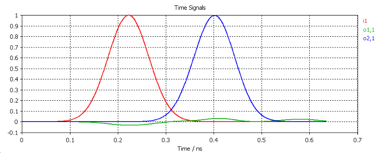
This plot shows the incident, reflected and transmitted wave amplitudes at the ports versus time. The incident wave amplitude is called i1 and the reflected or transmitted wave amplitudes of the two ports are o1,1 and o2,1. These curves show the delay in the transition from the input port to the output port and a relatively small reflection at the input port.
The S-Parameters can be plotted by clicking
on the 1D Results ![]() S-Parameters folder in the navigation tree.
S-Parameters folder in the navigation tree.
As expected, the input reflection S1,1 is quite small across the entire frequency range.
o 2D and 3D Results (Port Modes and Field Monitors)
Finally, you can observe the 2D and
3D field results. You should first inspect the port modes that can
be easily displayed by opening the 2D/3D Results ![]() Port
Modes
Port
Modes ![]() Port1 folder
from the navigation tree. To visualize the electric field of the
port mode, please click on the e1 folder. After properly
rotating the view you should obtain a plot similar to the following picture:
Port1 folder
from the navigation tree. To visualize the electric field of the
port mode, please click on the e1 folder. After properly
rotating the view you should obtain a plot similar to the following picture:
The plot also displays some important properties of the mode, such as mode type, propagation constant and line impedance. The port mode at the second port can be visualized in the same manner.
The three-dimensional surface current
distribution on the conductors can be shown by selecting one of the entries
in the 2D/3D Results ![]() Surface Current folder from the navigation tree.
The surface current at a frequency of 2 GHz can thus be visualized by
clicking at the 2D/3D Results
Surface Current folder from the navigation tree.
The surface current at a frequency of 2 GHz can thus be visualized by
clicking at the 2D/3D Results ![]() Surface Current
Surface Current ![]() surface current (f=2) [1] entry:
surface current (f=2) [1] entry:
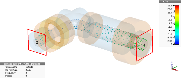
You can toggle an animation of the currents
on and off by selecting the Result Tools ![]() 2D/3D Plot
2D/3D Plot ![]() Animate Fields item. The surface currents for the other frequencies
can be visualized in the same manner.
Animate Fields item. The surface currents for the other frequencies
can be visualized in the same manner.
The transient S-Parameter calculation is primarily affected by two sources of numerical inaccuracies:
1. Numerical truncation errors introduced by the finite simulation time interval.
2. Inaccuracies arising from the finite mesh resolution.
In the following section, we provide hints on how to minimize these errors and achieve highly accurate results.
o Numerical Truncation Errors Due to Finite Simulation Time Intervals
As a primary result, the transient solver calculates the time varying field distribution that results from excitation with a Gaussian pulse at the input port. Thus, the signals at ports are the fundamental results from which the S-Parameters are derived using a Fourier Transform.
Even if the accuracy of the time signals themselves is extremely high, numerical inaccuracies can be introduced by the Fourier Transform that assumes the time signals have completely decayed to zero at the end. If the latter is not the case, a ripple is introduced into the S-Parameters that affects the accuracy of the results. The amplitude of the excitation signal at the end of the simulation time interval is called truncation error. The amplitude of the ripple increases with the truncation error.
Please note that this ripple does not move the location of minima or maxima in the S-Parameter curves. Therefore, if you are only interested in the location of a peak, a larger truncation error is tolerable.
The level of the truncation error can be controlled using the Accuracy setting in the transient solver control dialog box. Because increasing the accuracy requirement for the simulation limits the truncation error and in turn increases the simulation time, the accuracy requirement should be specified with care. As a general rule, the following table can be used:
|
Desired Accuracy Level |
Accuracy Setting (Solver control dialog box) |
|
Moderate |
-30dB |
|
High |
-40dB |
|
Very high |
-50dB |
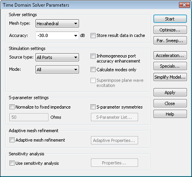
Default accuracy is -30dB, for typical coaxial connector devices a good compromise between speed and accuracy is -40dB. However, you may set the accuracy to -50dB or even -60dB with relatively little increase in computation time. For the following steps, please set the accuracy limit to -40dB.
The following rule may be useful as well: If you find a large ripple in the S-Parameters, increase the solvers accuracy setting.
o Effect of the Mesh Resolution on the S-Parameter Accuracy
Inaccuracies arising from the finite mesh resolution are usually more difficult to estimate. The only way to ensure the accuracy of the solution is to increase the mesh resolution and recalculate the S-Parameters. If these results no longer significantly change when the mesh density is increased, then convergence has been achieved.
In the example above, you have used
the default mesh that has been automatically generated by the expert system.
The easiest way to test the accuracy of the results is to use the fully
automatic mesh adaptation that can be switched on by checking the Adaptive
mesh refinement option in the Time
Domain Solver Parameters dialog box Home:
Simulation ![]() Start Simulation
Start Simulation ![]() Time Domain Solver
Time Domain Solver ![]() :
:
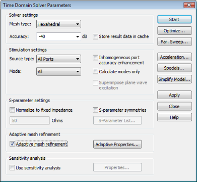
After activating the adaptive mesh refinement tool, you should now start the solver again by pressing the Start button. After a couple of minutes (during which the solver is running through mesh adaptation passes), the following dialog box will appear:
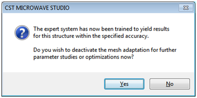
This dialog box informs you that the desired accuracy limit (2% by default) could be met by the adaptive mesh refinement. Because the expert systems settings have now been adjusted such that this accuracy is achieved, you may switch off the adaptation procedure for subsequent calculations (e.g. parameter sweeps or optimizations).
You should now confirm the deactivation of the mesh adaptation by pressing the Yes button.
After the mesh adaptation procedure is complete,
you can visualize the maximum difference of the S-Parameters for two subsequent
passes by selecting 1D Results
![]() Adaptive Meshing
Adaptive Meshing
![]() Delta S from
the navigation tree:
Delta S from
the navigation tree:
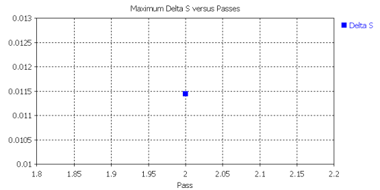
As evidenced in the above plot, only two passes of the mesh refinement were required to obtain highly accurate results within the given accuracy level that is set to 2% by default.
The
convergence process of the input reflection S1,1 during the mesh adaptation
can be visualized by selecting 1D Results ![]() Adaptive Meshing
Adaptive Meshing ![]() S-Parameters
S-Parameters ![]() S1,1 from the navigation
tree:
S1,1 from the navigation
tree:
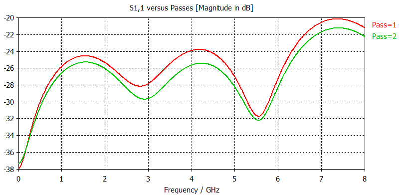
Please check the 1D plot, compare your result
with picture above, it is plotted in dB. If your plot is some other type,
select 1D Plot:
Plot Type ![]() dB
dB ![]() .
.
The major advantage of this expert system based mesh refinement procedure over traditional adaptive schemes is that the mesh adaptation needs to be carried out only once for each device to determine the optimum settings for the expert system. There is then no need for time consuming mesh adaptation cycles during parameter sweeps or optimization.
CST MICROWAVE STUDIO offers a variety of frequency domain solvers that are specialized for different types of problems. They differ not only by their algorithms but also by the grid type they are based on. The general purpose frequency domain solvers are available for hexahedral grids as well as for tetrahedral grids. The availability of a frequency domain solver within the same environment offers a very convenient way to cross-check results produced by the time domain solver with minimal additional effort.
o Making a Copy of Transient Solver Results
Before performing a simulation with a frequency domain solver, you may want to keep the results of the transient solver in order to compare the two simulations. The copy of the current results is obtained as follows: Select the S-Parameters folder in 1D Results and press Ctrl+c, afterwards press Ctrl+v on a newly created folder (select Add new tree folder from the context menu to create an extra folder). The copies of the results will be created in the selected folder. You may rename them to S1,1_TD, S2,1_TD and so on using the Rename command from the context menu. Please note that at the current time it is not possible to make a copy of 2D or 3D results.
o Frequency Domain Solver Settings
The
Frequency Domain Solver Parameters dialog box is opened by selecting Home:
Simulation ![]() Start Simulation
Start Simulation ![]() Frequency
Domain Solver
Frequency
Domain Solver ![]() .
.
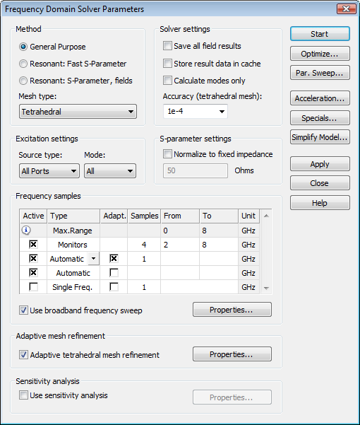
There are three different methods to choose from. For the example here, choose the General Purpose frequency domain solver. In the Mesh Type combo box you may choose between Hexahedral and Tetrahedral Mesh. Please choose Tetrahedral Mesh.
S-Parameters in the frequency domain are obtained by solving the field problem at different frequency samples. These single S-Parameter values are then used by the broadband frequency sweep to get the continuous S-Parameter values. With the default settings in the Frequency samples frame the number and the position of the frequency samples are chosen automatically in order to fit the required accuracy limit throughout the entire frequency band.
Unlike the time domain solver, the tetrahedral frequency domain solver should always be used with the Adaptive tetrahedral mesh refinement. Otherwise, the initial mesh may lead to a poor accuracy. Therefore, the corresponding check box is activated by default.
All other settings may also be left unchanged. Press Start to begin the calculation.
There may be old results present from the previous transient solver run that will be overwritten when starting a different solver. In this case, the following warning message appears:
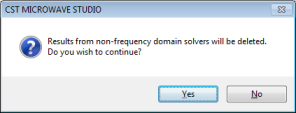
Press Yes to acknowledge the deletion. A progress bar and an abort button appear in the status bar showing information about the solver stages. After the desired accuracy for the S-Parameter has been reached, the simulation stops. When the simulation has finished or if it has been aborted, both items disappear again.
During the simulation, the Message Window will show some details about the performed simulation.
Congratulations, you have simulated the coaxial connector using the frequency domain solver! Lets review the results:
o 1D Results (S-Parameters)
You
can visualize the maximum difference of the S-Parameters for two subsequent
passes by selecting 1D Results ![]() Adaptive Meshing
Adaptive Meshing ![]() f=8
f=8 ![]() Delta S from the navigation tree:
Delta S from the navigation tree:
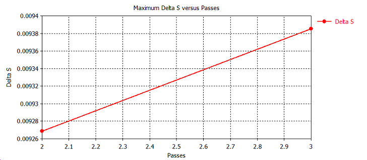
As evident in the above plot, only three passes of the mesh refinement were required to obtain highly accurate results within the given accuracy level, which is set to 1% by default.
You
can view the S-Parameters by selecting 1D Results ![]() S-Parameters in the navigation
tree.
S-Parameters in the navigation
tree.
As expected, the input reflection S1,1 is quite small across the entire frequency range.
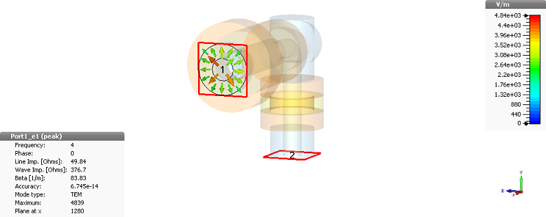
o 2D and 3D Results (Port Modes and Field Monitors)
Finally,
you can observe the 2D and 3D field results. You should first inspect
the port modes that can be easily displayed by opening the 2D/3D Results
![]() Port Modes
Port Modes ![]() Port1 folder from the navigation tree.
To visualize the electric field of the port mode, please click on the
e1 folder. Open the Select Port Mode dialog box by selecting
Results
Port1 folder from the navigation tree.
To visualize the electric field of the port mode, please click on the
e1 folder. Open the Select Port Mode dialog box by selecting
Results ![]() Select Mode Frequency from the main menu and change the
frequency to 4 GHz. Please confirm your setting by pressing OK.
After properly rotating the view, you should obtain a plot similar to
the following picture:
Select Mode Frequency from the main menu and change the
frequency to 4 GHz. Please confirm your setting by pressing OK.
After properly rotating the view, you should obtain a plot similar to
the following picture:
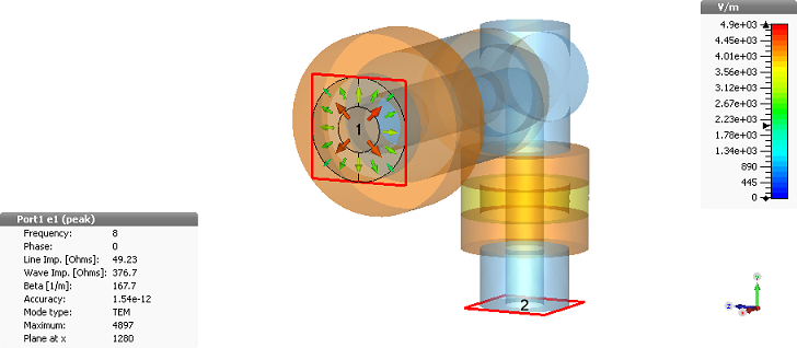
The plot also shows some important properties of the mode, such as mode type, propagation constant and line impedance. The port mode at the second port can be visualized in the same manner.
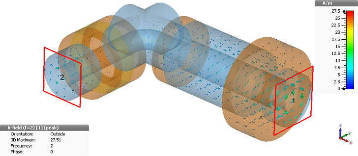
The
three-dimensional h-field distribution can be displayed by selecting one
of the entries in the 2D/3D Results ![]() H-Field folder from the navigation
tree. The magnetic field at a frequency of 2 GHz can thus be visualized
by clicking at the 2D/3D Results
H-Field folder from the navigation
tree. The magnetic field at a frequency of 2 GHz can thus be visualized
by clicking at the 2D/3D Results ![]() H-Field
H-Field ![]() h-field (f=2)
[1] entry:
h-field (f=2)
[1] entry:
You
can toggle an animation of the currents on and off by selecting Result
Tools ![]() 2D/3D Plot
2D/3D Plot ![]() Animate Fields.
The surface currents for the other frequencies can be visualized in the
same manner, as shown above.
Animate Fields.
The surface currents for the other frequencies can be visualized in the
same manner, as shown above.
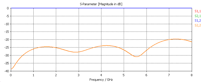
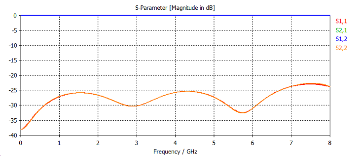
The next plot shows the S-Parameters S1,1 and S1,2 resulting from the time domain and frequency domain simulations. Plotting the S-Parameter curves in the same graph allows for a better comparison.
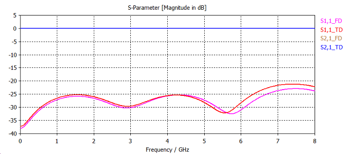
As you can see, the results agree very well. Since the results are not converged to the highest possible accuracy level, there is still a slight difference between the curves. When refining the accuracy limit in the adaptive mesh refinement the difference will become negligible.
Congratulations! You have just completed the Coaxial Structure tutorial that should have provided you with a good working knowledge on how to use CST MICROWAVE STUDIO to calculate S-Parameters. The following topics have been covered:
1. General modeling considerations, using templates, etc.
2. Model a coaxial structure using the rotate, cylinder and extrude tools and define the substrates.
3. Define ports.
4. Define frequency range, boundary conditions and symmetry planes.
5. Define field monitors for surface current distributions.
6. Start the transient or the frequency domain solver.
7. Visualize port signals and S-Parameters
8. Visualize port modes and surface currents.
9. Check the truncation error of the time signals
10. Obtain accurate and converged results using the automatic expert system based mesh adaptation.
You can obtain more information for each particular step from the online help system that can be activated either by pressing the Help button in each dialog box or by pressing the F1 key at any time to obtain context sensitive information.
In some cases we have referred to the CST MICROWAVE STUDIO Workflow and Solver Overview or CST STUDIO SUITE Getting Started manuals, they are also a good source of information for general topics.
In addition to this tutorial, you can find some more S-Parameter calculations in the examples folder in your installation directory. Each of these examples contains a Readme item in the navigation tree that will give you some more information about the particular device.
Finally, you should refer to the Online documentation for more in depth information on issues such as the fundamental principles of the simulation method, mesh generation, usage of macros to automate common tasks, etc.
And last but not least: Please also visit one of the training classes held regularly at a location near you. Thank you for using CST MICROWAVE STUDIO!


HFSSЪгЦЕНЬГЬ ADSЪгЦЕНЬГЬ CSTЪгЦЕНЬГЬ Ansoft Designer жаЮФНЬГЬ
|
Copyright © 2006 - 2013 ЮЂВЈEDAЭј, All Rights Reserved вЕЮёСЊЯЕЃКmweda@163.com |
|