|
|
|
| �� | |
| �� | |
| ��ҳ >> CST�̳� >> CST2013���߰���ϵͳ |
Signal Integrity: Simulation of Via ModelTutorials
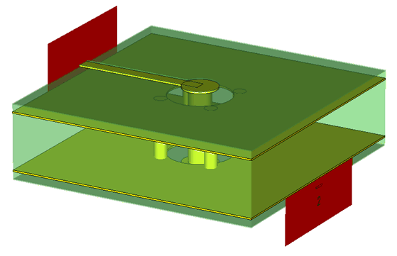
Abstract The miniaturization and the large-scale integration of electronic devices place increasing demand on the multilayer interconnect geometry. The layout of printed circuit boards (PCBs) involves a large number of discontinuities, and their presence causes signal distortion and all the related problems for the mounted digital devices. For this reason an accurate modeling of discontinuities at PCB level is essential for signal integrity (SI) analysis. A methodology is presented in this tutorial for the analysis and the characterization of a simple via hole in multilayer PCB. ContentsIntroductionPhysical DescriptionIn general, signal integrity refers to the quality of an electrical signal or pulse on the interconnect track of a PCB or component. Electronic signals, particularly high speed signals will deteriorate, distort or oscillate if the designer has not made allowances for impedance matching and signal transmission effects. In other words, signal integrity refers to electronic circuit tools and techniques which ensure that electrical signals are of sufficient quality for proper operation. Alternatively, signal integrity tools attempt to identify and remove effects that cause a design to malfunction due to distortion of the signal wave forms. The main cause of signal integrity problems is noise induced by neighboring connections, or cross-talk. CST MICROWAVE STUDIO Model
|
|
|
|
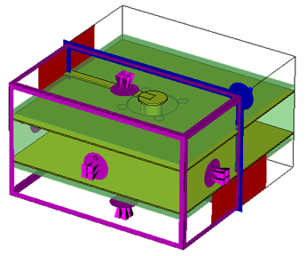
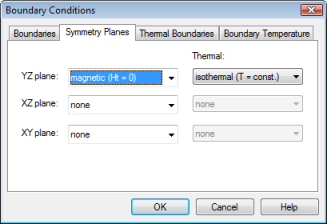
Figure 3 - Boundary condition settings
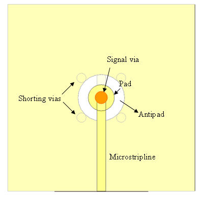
Particular attention has been given to the excitation: the two ”ports” at which the electrical fields and the S-parameters are evaluated are the upper surface of the microstriplines. In order to ensure a TEM structure of the electromagnetic field (essential condition for a meaningful interpretation of the scattering matrix), lumped voltage sources are not suitable because they would excite higher order modes. Because of this, the TEM excitation has been given by considering fictitious wave guide structures (named waveguide port) that cause a TEM or quasi-TEM structure of the field at these planes. Figure 4 depicts the mode pattern, the Beta, the line impedance as well as the wave impedance value.
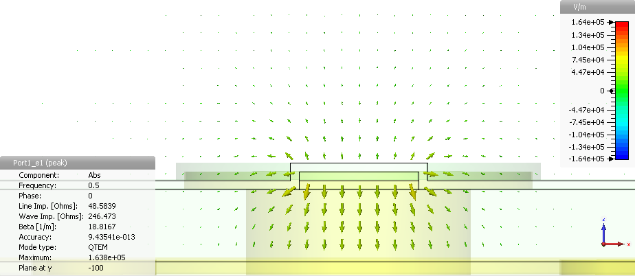
Figure 4 - Port mode plotting
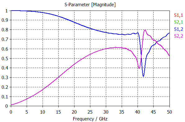
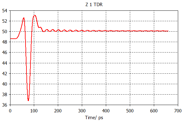
The S-parameters (in the range 0-50GHz) and the TDR are evaluated, and the wave forms are reported in Figure 5. These informations are of main interest for SI device characterization since they allow the design engineer to have an overview of both time and frequency domain performance.
|
|
|
Figure 5 - S-parameters and TDR
In addition a time domain monitor can be used to analyze and visualize the transient field distribution in the device as shown in the following picture:
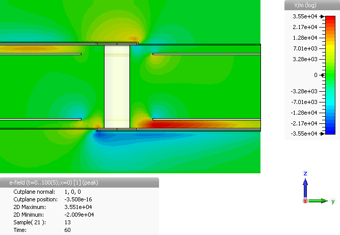
Figure 6 - Z component of the electric field in logarithmic scaling
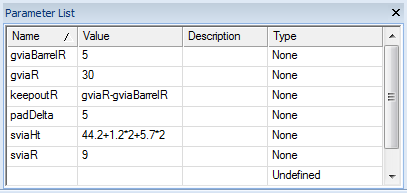
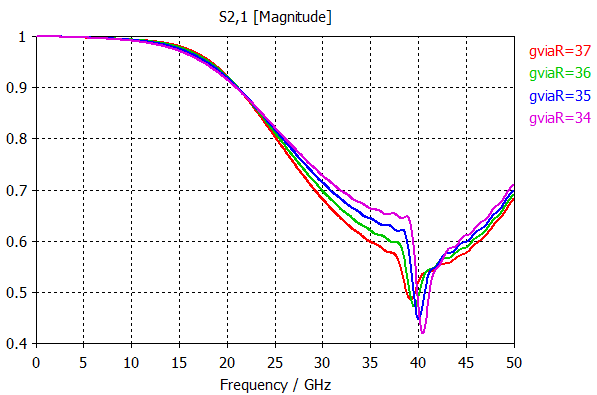
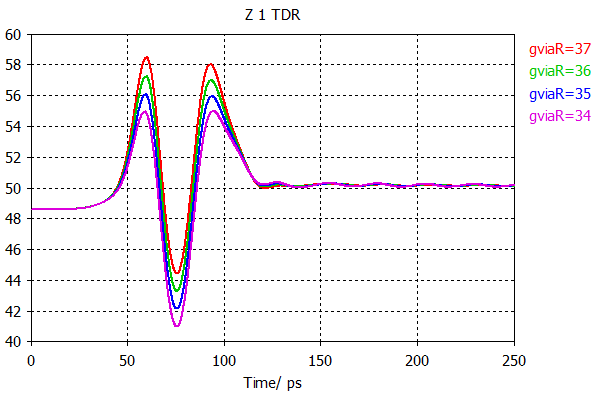
At this point, a parameter sweep (see Figure 7) for the via antipad radius is performed in order to study the impact on the general performance of the model. The parameters have been defined so that the shorting vias are automatically adjusted in their position to the new value of the antipad. Insertion loss and TDR are illustrated in Figure 8.

Figure 7 - Parameter sweep dialog and settings
|
|
|
Figure 8 - Insertion loss and TDR due to the variation of the antipad radius (gviaR)
Important considerations can be addressed:
By increasing the radius of the antipad the insertion loss gets worse.
By increasing the radius of the antipad the TDR impedance presents a larger deviation from the nominal value.
A common assumption in designing vias in PCBs is that by increasing the antipad radius there is an improvement on the insertion loss. The different behavior which is observed in the present example is because of the presence of the shorting vias whose distance from the signal via is automatically increased with the increased value of the antipad radius. Therefore, a different return path to the current is provided.
This simple study shows the importance of the 3D full wave simulation when dealing with PCB discontinuities and high frequencies: even a simple structure (like a single-ended via hole with two short lines) can have unexpected results.


HFSS��Ƶ�̳� ADS��Ƶ�̳� CST��Ƶ�̳� Ansoft Designer ���Ľ̳�
|
Copyright © 2006 - 2013 ��EDA��, All Rights Reserved ҵ����ϵ��mweda@163.com |
|