![]()
![]()
|
Single Antenna (Transient Solver): |
|
|
Single Antenna (Frequency Domain Solver): |
|
|
Antenna Array (Transient Solver): |
|
|
Antenna Array Combine (Transient Solver): |
|
|
Antenna Array Simultaneous (Transient Solver): |
|

Introduction and Model Dimensions
S-Parameter and Farfield Calculation
Frequency Domain Solver Results
In this tutorial you will learn how to simulate antenna devices. As a typical example you will analyze a circular patch antenna. The following explanations can be applied to other antennas as well.
Although, CST MICROWAVE STUDIO can provide a wide variety of results, this tutorial will concentrate mainly on the S-parameters and farfield results.
In addition, the single patch antenna will be extended to a rectangular 2x2 array pattern using three different methods. First, the farfield solution of the single patch antenna is applied to the antenna array feature, superimposing the results with different amplitudes and phase settings. Another possibility expands the patch model to a set of four identical antennas, each excitable with its own coaxial feed. Here, you have the option to calculate the antennas separately one after another and finally combine the results with arbitrary amplitudes and phase values, or to run the excitation simultaneously to produce the farfield result with only one solver cycle. The farfield distributions of all these possibilities will be compared.
We strongly suggest that you carefully read through the CST MICROWAVE STUDIO Getting Started and CST MICROWAVE STUDIO Workflow and Solver Overview manual before starting this tutorial.

The structure depicted above consists of two different materials: the Substrate and the Perfect Electric Conductor (PEC). There is no need to model the air above because it will be added automatically (according to the current background material setting) when the open boundary conditions are specified. This will be done automatically with an appropriate template. The feeding of the patch is realized with a coaxial line.
This tutorial will take you step-by-step through the construction of your model, and relevant screen shots will be provided so that you can double-check your entries along the way.
Please remember the Undo ![]() facility in the event that you want to cancel the last construction
step.
facility in the event that you want to cancel the last construction
step.
o Create a New Project
After launching the CST STUDIO SUITE
you will enter the start screen showing you a list of recently opened
projects and allowing you to specify the application which suits your
requirements best. The easiest way to get started is to configure a project
template which defines the basic settings that are meaningful for your
typical application. Therefore click on the Create
Project button ![]() in the New Project
section.
in the New Project
section.
Next you should choose the application area, which is Microwaves & RF for the example in this tutorial and then select the workflow by double-clicking on the corresponding entry.

For the Patch Antenna structure, please
select Antennas ![]() Planar (Patch,
Slot, etc.)
Planar (Patch,
Slot, etc.)
![]() Time Domain Solver
Time Domain Solver ![]() .
.
At last you are requested to select the units which fit your application best. For the Patch Antenna structure, please select the dimensions as follows:
|
Dimensions: |
mm |
|
Frequency: |
GHz |
|
Time: |
ns |
For the specific application in this tutorial the other settings can be left unchanged. After clicking the Next button, you can give the project template a name and review a summary of your initial settings:
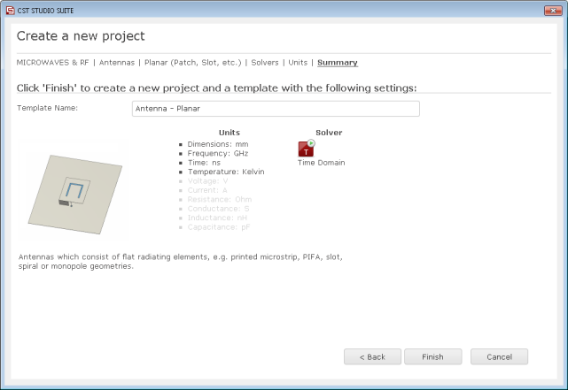
Finally click the Finish button to save the project template and to create a new project with appropriate settings. CST MICROWAVE STUDIO will be launched automatically due to the choice of the application area Microwaves & RF.
Please note: When you click again on the File: New and Recent you will see that the recently defined template appears below the Project Templates section. For further projects in the same application area you can simply click on this template entry to launch CST MICROWAVE STUDIO with useful basic settings. It is not necessary to define a new template each time. You are now able to start the software with reasonable initial settings quickly with just one click on the corresponding template.
Please
note: All settings made for a project template can be modified
later on during the construction of your model. For example, the units
can be modified in the units dialog box (Home:Settings ![]() Units
Units ![]() )
and the solver type can be selected in the Home:Simulation
)
and the solver type can be selected in the Home:Simulation ![]() Start Simulation drop-down
list.
Start Simulation drop-down
list.
o Set the Working Planes Properties
The
next step will usually be to set the working plane properties to make
the drawing plane large enough for your device. Because the structure
has a maximum extension of 60 mm along a coordinate direction, the working
plane size should be set to at least 100 mm. These settings can be
changed in a dialog box that opens after selecting View:Visibility ![]() Working Plane
Working Plane ![]()
![]() Working Plane
Properties. Please note that we will
use the same document conventions here as introduced in the Workflow and Solver Overview manual.
Working Plane
Properties. Please note that we will
use the same document conventions here as introduced in the Workflow and Solver Overview manual.
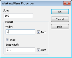
In this dialog box, you should set the Size to 100 (the unit which has previously been set to mm is displayed in the status bar), the Raster width to 2 and the Snap width to 0.1 to obtain a reasonably spaced grid. Please confirm these settings by pressing the OK button.
o Draw the Substrate Brick
The
first construction step for modeling a planar structure is usually to
define the substrate layer. This can be easily achieved by creating
a brick made of the substrates material. Please activate the brick creation
mode Modeling:
Shapes ![]() Brick
Brick ![]() .
.
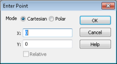
When you are prompted to define the first point, enter the coordinates numerically by pressing the Tab key that will open the following dialog box:

In this example, you should enter a substrate block that has an extension of 60 mm in each of the transversal directions. The transversal coordinates can thus be described by X = -30, Y = -30 for the first corner and X = 30, Y = 30 for the opposite corner, assuming that the brick is modeled symmetrically to the origin. Thus, please enter the first points coordinates X = -30 and Y = -30 in the dialog box and press the OK button.
Afterwards, you can repeat these steps for the second point:
1. Press the Tab key
2. Enter X = 30, Y = 30 in the dialog box and press OK.
Now you will be requested to enter the height of the brick. This can also be numerically specified by pressing the Tab key again, entering the Height of -0.7 and pressing the OK button (it is convenient to define the substrate in the negative z-direction). Now the following dialog box will appear, displaying a summary of your previous input:
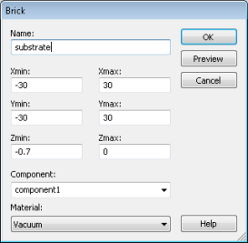
Please check all these settings carefully. If you encounter any mistakes, please change the value in the corresponding entry field.
You should now assign a meaningful name to the brick by entering e.g. substrate in the Name field, keep the Component default setting (component1).
Please note: The use of different components allows you to combine several solids into specific groups, independent of their material behavior. However, in this tutorial, it is convenient to construct the single patch antenna as a representation of one component that can then easily be extended into a patch antenna array.
Finally, you need to define the substrate material. Because no material has yet been defined for the substrate, you should open the New Material Parameters dialog box by selecting [New Material...] from the Material dropdown list:
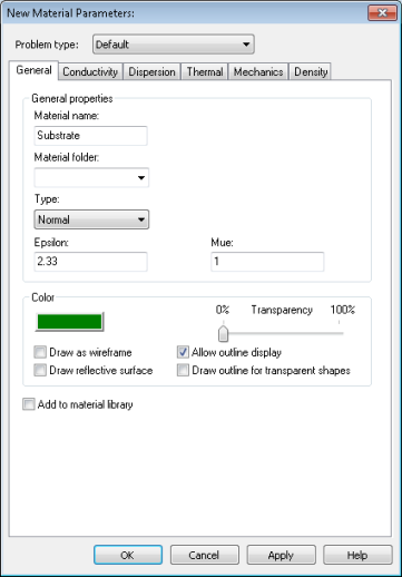
In this dialog box, define a new Material name (e.g. Substrate) and set the Type to a Normal dielectric material. Afterwards, specify the material properties in the Epsilon and Mue fields. Here, you only need to change the dielectric constant Epsilon to 2.33. Finally, choose a color for the layer by pressing the Change button. Your dialog box should now look similar to the above picture before you press the OK button.
Please note: The defined
material Substrate will now be available inside the current project for
the further creation of other solids. However, if you want to also
save this specific material definition for other projects, you may check
the button Add to material library. You will have access
to this material database by clicking on Modeling:
Materials ![]() Material Library
Material Library ![]()
![]() Load from Library .
Load from Library .
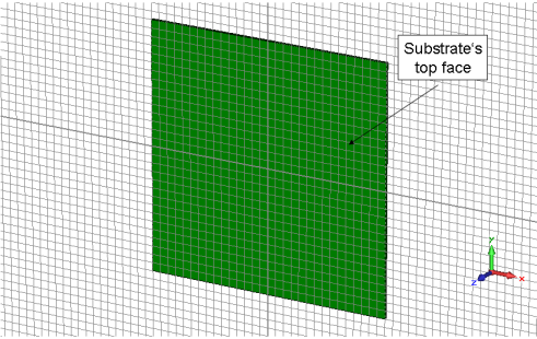
Back in the brick creation dialog box you can also press the OK button to finally create the substrate brick. Your screen should now look as follows (you can press the Space bar in order to zoom the structure to the maximum possible extent):
o Model the Ground Plane
The
next step is to model the ground plane of the patch antenna. Because the
antenna will be excited by a coaxial feed at the bottom face, the electric
boundary at Zmin defined by the previously chosen template is not
suitable as a ground plane. Consequently, a metallic brick must be additionally
defined. First, the model has to be rotated by activating the rotation
mode View:
Mouse Control ![]() Rotate
Rotate ![]() . Then the bottom
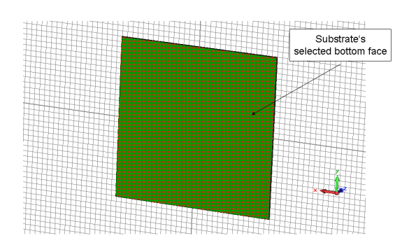
face has to be activated by the face pick tool Modeling:
Picks
. Then the bottom
face has to be activated by the face pick tool Modeling:
Picks ![]() Picks
Picks ![]()
![]() Pick Points,
Edges or Faces double-clicking
on the substrates bottom face. The face selection should then be visualized
as follows:
Pick Points,
Edges or Faces double-clicking
on the substrates bottom face. The face selection should then be visualized
as follows:
You
can now extrude the selected face with the Extrude tool selecting
Modeling:
Shapes ![]() Extrude
Extrude ![]() . Here, you must enter the height and the
material of the new shape to be created. In this example, the ground plane
must have a non-zero thickness because of the coaxial feed that will be
modeled later. In CST MICROWAVE STUDIO a port region must be homogeneous
for at least three mesh lines in longitudinal direction. You can therefore
choose a Height of 2.1 mm, representing three times the substrate
thickness, as a sufficient dimension. Enter this value in the following
dialog box and select PEC from the Material dropdown list as the
metallic material property:
. Here, you must enter the height and the
material of the new shape to be created. In this example, the ground plane
must have a non-zero thickness because of the coaxial feed that will be
modeled later. In CST MICROWAVE STUDIO a port region must be homogeneous
for at least three mesh lines in longitudinal direction. You can therefore
choose a Height of 2.1 mm, representing three times the substrate
thickness, as a sufficient dimension. Enter this value in the following
dialog box and select PEC from the Material dropdown list as the
metallic material property:

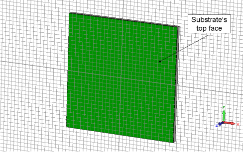
After entering a suitable name (e.g. ground) in the Name field and confirming your settings with the OK button, the current structure will look like this (rotated again to the see the top face):
o Model the Patch Antenna
After the ground plane has been defined, the patch antenna
must be modeled as a cylindrical shape on the substrates top face. Please
activate the cylinder creation mode Modeling:
Shapes ![]() Cylinder
Cylinder ![]() . Similar to the construction of the
substrates brick, enter the coordinates numerically by pressing the Tab
key to open the following dialog box:
. Similar to the construction of the
substrates brick, enter the coordinates numerically by pressing the Tab
key to open the following dialog box:
Here,
enter the center point of the cylinder with X = 0 and Y = 0 because the
patch is located symmetrically on the substrate. Afterwards, please define
the Radius with
23.2 mm and the Height with 0.07 mm in the shown dialog boxes that
appear after you have pressed the Tab button:
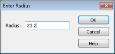

Skipping the entry dialog for the inner radius by pressing the Esc button will lead to the following dialog box that provides a summary of your entered parameters:
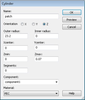
Select PEC as the Material setting for the patch and assign a meaningful name to the brick by entering e.g. patch in the Name input field.
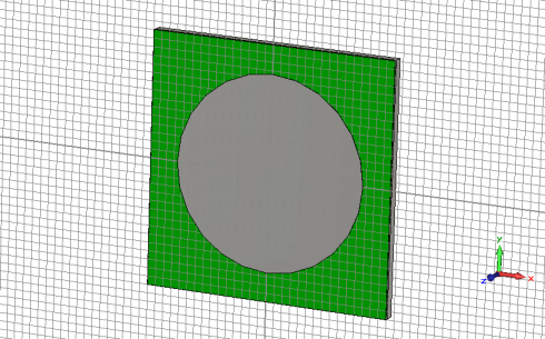
Again, please check the settings carefully and change any mistakes in the corresponding entry field. After you apply the settings with the OK button, your screen should show the following structure:
o Model the Coaxial Feed
The
last modeling step is the construction of the coaxial feed as the excitation
source for the patch antenna. This action introduces the working coordinate
system (WCS). Because the feeding point is located asymmetrical to the
circular patch it is advisable to activate the local coordinate system
Modeling:
WCS![]() Local
WCS
Local
WCS ![]() .
.
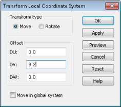
To
define the new center point for the coaxial feed the local coordinate
system is moved along the positive v-direction Modeling:
WCS![]() Transform WCS
Transform WCS ![]() .
Therefore, please enter a value of 9.2 mm in the following dialog box:
.
Therefore, please enter a value of 9.2 mm in the following dialog box:
Now it is possible to design the coaxial feed by constructing two cylindrical shapes, similar to the previously defined circular patch.
Please
activate the cylinder creation mode again (tool Modeling:
Shapes ![]() Cylinder
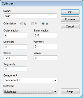
Cylinder ![]() ). First, enter the values for the coaxial substrate
cylinder using the Tab key, again skipping the input of the inner
radius. The cylinder has an outer radius of 4 mm and an extension in the
negative w-direction of 2.1+0.7=2.8 mm. Select the previously defined
Substrate material from the Material dropdown list. Please check
your settings against the following dialog box and then create the cylinder
with the OK button:
). First, enter the values for the coaxial substrate
cylinder using the Tab key, again skipping the input of the inner
radius. The cylinder has an outer radius of 4 mm and an extension in the
negative w-direction of 2.1+0.7=2.8 mm. Select the previously defined
Substrate material from the Material dropdown list. Please check
your settings against the following dialog box and then create the cylinder
with the OK button:
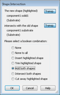
As a result, the cylinder shape component1:solid1 intersects with two already existing shapes, the solid component1:substrate and the ground plane component1:ground. Here it is necessary to determine the type of intersection for the shapes. It is more convenient to combine the two substrate materials into a single shape, so please mark the radio button Add both shapes in the Shape Intersection dialog box as presented below and confirm with OK:
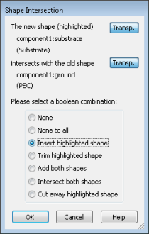
In the second case, the substrate cylinder must be inserted into the PEC material of the ground plane. Please mark the radio button Insert highlighted shape from the Shape Intersection dialog window as presented below and confirm again with OK:
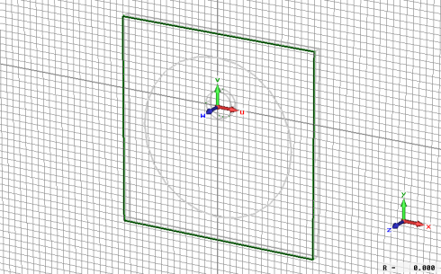
The
following screenshot allows you to double-check your model (please use
Ctrl+w or View:Visibility ![]() Wire Frame
Wire Frame ![]() to toggle
the wireframe visualization mode on and off):
to toggle
the wireframe visualization mode on and off):
The inner conductor is constructed by defining another cylinder made of PEC material. Please define the cylinder with an outer radius of 1.12 mm and again an extension of 2.8 mm in the negative w-direction in a similar way as before. This time, select PEC from the Material dropdown list and define again a suitable name (e.g. feed) for the cylinder shape. Create the cylinder by pressing the OK button.
Please note: In this case no Shape intersection dialog window will appear, because the PEC shape is defined after the normal material shape (here: Substrate). This implies that the PEC shape is automatically inserted into the intersected shape. Refer to the Workflow and Solver Overview manual for more details.
After
applying the OK button the final model will look like the below
figure (again use Ctrl+w or View:Visibility ![]() Wire Frame
Wire Frame ![]() to toggle the wireframe visualization mode on and off):
to toggle the wireframe visualization mode on and off):

To this point, only the structure itself has been modeled. Now it is necessary to define some solver-specific elements. For an S-parameter calculation you must define input and output ports. Furthermore, the simulation needs to know how the calculation domain should be terminated at its bounds.
o Define the Waveguide Port
The next step is to add the excitation port to the patch antenna device, for which the reflection parameter will later be calculated. The port simulates an infinitely long coaxial waveguide structure that is connected to the structure at the ports plane.
A waveguide port extends the structure to infinity. Its transversal extension must be large enough to sufficiently cover the corresponding modes. In contrast to open port structures, the port range in this case is clearly defined by the outer shielding conductor of the coaxial waveguide.
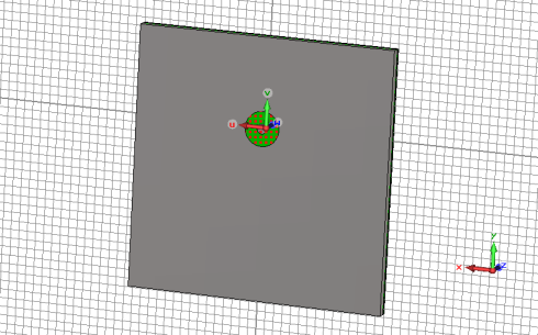
Consequently,
the easiest way to define the port range is to pick the face (pick tool
Modeling:
Picks ![]() Picks
Picks ![]()
![]() Pick Points,
Edges or Faces) of the coaxial feed (Substrate
material) as demonstrated below (the model is rotated again to the bottom
side first):
Pick Points,
Edges or Faces) of the coaxial feed (Substrate
material) as demonstrated below (the model is rotated again to the bottom
side first):
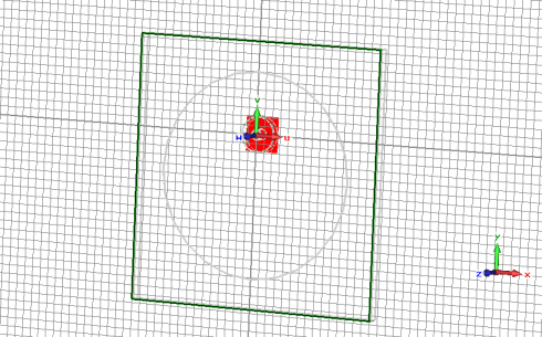
Please
now open the waveguide dialog box (Simulation:
Sources
and Loads ![]() Waveguide Port
Waveguide Port ![]() ) to define the port:
) to define the port:
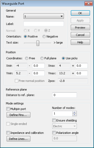
Here, you have to choose how many modes should be considered by the port. For a simple coax port with only one inner conductor, usually only the fundamental TEM mode is of interest. Thus, you should simply keep the default setting of one mode.
Please confirm your port settings with the OK button to finally create the port. After rotating the model again to the top face, your model should now look as follows (please use again Ctrl+w to toggle the wireframe visualization mode on and off):
o Define the Frequency Range
The frequency range for the simulation should be chosen with care. Different considerations must be made when using a transient solver or a frequency domain solver (see next chapter for details).
In
this example, the S-parameters are to be calculated for a frequency range
between 2 and 3 GHz. Open the frequency range dialog box (Simulation:
Frequency
and Boundaries ![]() Frequency
Frequency
![]() )
and enter the range from 2 to 3 (GHz) before pressing the OK
button (the frequency unit has previously been set to GHz and is displayed
in the status bar):
)
and enter the range from 2 to 3 (GHz) before pressing the OK
button (the frequency unit has previously been set to GHz and is displayed
in the status bar):

o Boundary Conditions
Because
the calculation domain is only a limited volume it is necessary to define
boundary conditions that incorporate the influences of the outer space.
Please open the Boundary Conditions dialog box by selecting (Simulation:
Frequency
and Boundaries ![]() Boundaries and Symmetries
Boundaries and Symmetries ![]() ),
where all currently
selected boundary conditions are simultaneously displayed in the main
view:
),
where all currently
selected boundary conditions are simultaneously displayed in the main
view:
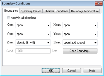
At the ground plane, an electric boundary condition has to be set that behaves like an infinite solid PEC brick. All other boundary planes are set to open or open (add space); they realize free space behind their boundary planes. Free space means that the electromagnetic fields are absorbed at these boundaries with virtually no reflections as if they propagate in infinite empty space.
Please note: As a general rule, the open boundary conditions work best if they are at least 1/8 wavelength apart from the field source. Open (add space) already incorporates this rule and automatically adds the correct amount of background space to the structure.
Because the open (add space) boundary condition only adds background material to the structure, it should not be used if there is material that crosses the boundary plane and should practically extend to infinity (such as the substrate and ground solids in this example). In these cases, the open boundary condition must be invoked.
Please close this dialog box without any further changes.
o Define Farfield Monitor
Besides the S-parameters, the main result of interest for antenna devices is the farfield distribution at a given frequency. The solvers in CST MICROWAVE STUDIO offer the possibility of defining several field monitors to specify at which frequencies the field data shall be stored.
Please open the monitor definition dialog box by selecting
Simulation:
Monitors
![]() Field Monitor
Field Monitor
![]() :
:
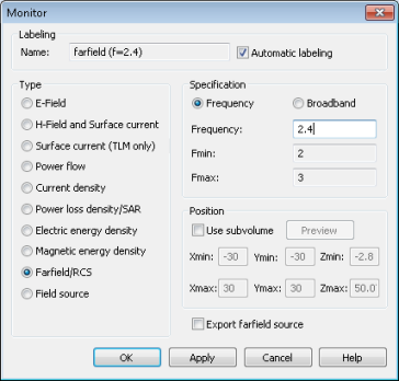
In this dialog box, you should first select the Type Farfield/RCS before specifying the frequency for this monitor in the Frequency field. Afterwards, press the Apply button to store the monitors data. Please define a monitor at the frequency of 2.4 (with GHz being the currently active frequency unit). However, you may define additional monitors at other frequencies, each time pressing the Apply button to confirm the setting and add the monitor in the Monitors folder in the navigation tree. After the monitor definition is complete, please close this dialog box by pressing the OK button.
A key feature of CST MICROWAVE STUDIO is the Method on Demand approach that allows specification of a simulator or mesh type that is best suited to a particular problem. Another benefit is the ability to compare the results from completely independent approaches. We demonstrate this strength in the following two paragraphs by calculating the S-parameters and the farfield of the constructed antenna device with both the transient and frequency domain solvers. The transient simulation uses a hexahedral mesh while the frequency domain calculation is performed with a tetrahedral mesh in this case. However, because both methods are self-contained, it is sufficient to work through only one of them. The chapter ends with a comparison of the two methods.
Please note that not all solvers may be available to you due to license restrictions. Please contact your sales office for more information.
o Frequency Range Considerations for the Transient Solver
We recommend using reasonably large bandwidths of 20% to 100% for the transient simulation. In this example, the S-parameters are to be calculated for a frequency range between 2 and 3 GHz. With a center frequency of 2.5 GHz, the bandwidth (3 GHz - 2 GHz = 1 GHz) is 40% of the center frequency, which is inside the recommended interval. Thus, you can simply choose the frequency range as desired between 2 and 3 GHz.
Please note: a) In a case where you just cover a bandwidth of less than 20%, you can increase the frequency range without losing accuracy. This extension of the frequency range could speed up your simulation by more than a factor of three!
b) In contrast to frequency domain solvers, the lower frequency can be set to zero without any problems! The calculation time can often be reduced by half if the lower frequency is set to zero rather than e.g. 0.01 GHz.
o Transient Solver Settings
The solver parameters are specified in the Transient Solver
Parameters dialog box that can be opened by selecting Home:
Simulation ![]() Start Simulation
Start Simulation ![]() Time Domain Solver
Time Domain Solver ![]() :
:
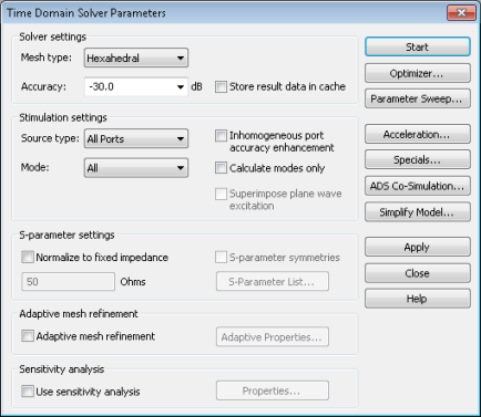
You can accept the default settings and press the Start button to run the calculation. A progress bar appears at the bottom of the main window, displaying information about the calculations status. This progress window disappears when the solver has successfully finished.
![]()
During the simulation, the Message Window will show some details about the performed simulation.
Please note: If there are any warning or error messages during the simulation they will be written into the message window, as well.
Congratulations, you have simulated the circular patch antenna using the transient solver! Lets review the results.
o 1D Results (Port Signals, S-Parameters)
First, observe the port signals. Open the 1D Results folder in the navigation tree and click on the Port signals folder.
Please note: It is possible to observe the progress of the results during the computation. In order to get the complete information, however, wait until the solver has finished.
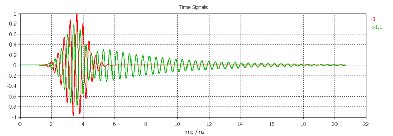
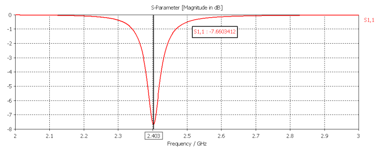
This plot shows the incident and reflected wave amplitudes at the waveguide port versus time. The incident wave amplitude is called i1 (referring to the port name: 1) and the reflected wave amplitude is o1,1. As evident from the above time-signal plot, the patch antenna array has a strong resonance that leads to a slowly decreasing output signal.
A primary result for the antenna is the S11 parameter that
will appear if you click on the 1D Results ![]() S Parameters folder from the navigation
tree and selecting 1D Plot:
Plot Type
S Parameters folder from the navigation
tree and selecting 1D Plot:
Plot Type
![]() dB
dB ![]() .
The following screenshot shows the reflection parameter:
.
The following screenshot shows the reflection parameter:
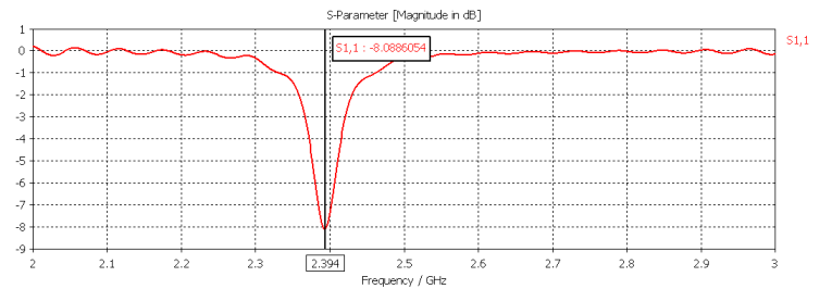
It
is possible to precisely determine the operational frequency for the patch
antenna. Activate the axis marker by pressing 1D Plot:
Markers
![]() Axis
Marker
Axis
Marker ![]() or by pressing the right mouse button and selecting the Show
Axis Marker option from the context menu. Now you can move
the marker to the S11 minimum and pinpoint a resonance frequency for the
patch antenna of about 2.4 GHz.
or by pressing the right mouse button and selecting the Show
Axis Marker option from the context menu. Now you can move
the marker to the S11 minimum and pinpoint a resonance frequency for the
patch antenna of about 2.4 GHz.
The ripples that appear in the reflection parameters result from the time signal not sufficiently decaying (review again at the time signal plot). The amplitude of the ripples increases with the signal amplitude remaining at the end of the transient solver run. However, these ripples do not affect the location of the resonance frequency and therefore can be ignored for this example. More information about this type of numerical error is available in the Accuracy Considerations chapter.
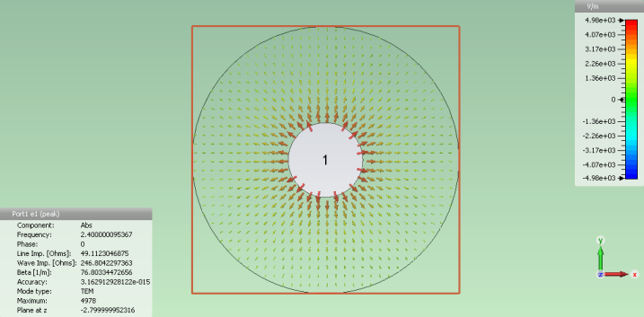
o 2D and 3D Results (Port Modes and Farfield Monitors)
You should first inspect the port modes that
can be easily displayed by opening the 2D/3D Results ![]() Port
Modes
Port
Modes ![]() Port1 folder from the navigation tree. To visualize
the electric field of the fundamental port mode, click on the e1
folder. After properly rotating the view and tuning some settings in the
plot properties dialog box, you should obtain a plot similar to the following
picture (please refer to the Workflow and Solver Overview manual for more information on how to change the plots parameters):
Port1 folder from the navigation tree. To visualize
the electric field of the fundamental port mode, click on the e1
folder. After properly rotating the view and tuning some settings in the
plot properties dialog box, you should obtain a plot similar to the following
picture (please refer to the Workflow and Solver Overview manual for more information on how to change the plots parameters):
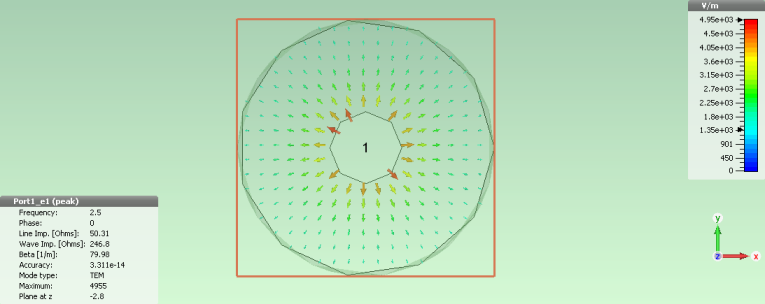
The plot also shows some important properties of the coaxial mode such as TEM mode type, propagation constant and line impedance, etc.
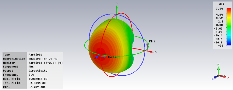
In addition to the resonance frequency, the farfield is another important parameter in antenna design.
The farfield solution of the antenna device
can be shown by selecting the corresponding monitor entry in the Farfields
folder from the navigation tree. For example, the farfield at the frequency
2.4 GHz can be visualized by clicking on the Farfields ![]() farfield (f=2.4)
[1] entry, showing the directivity over the phi and theta angle:
farfield (f=2.4)
[1] entry, showing the directivity over the phi and theta angle:
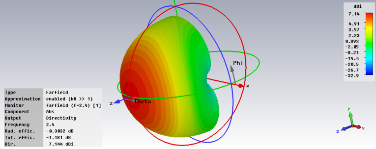
Please note:
You have the option to change FarField Plot:
Plot Properties![]() Properties
Properties
![]() angle step to 5 degrees for a better angle accuracy of the plot.
angle step to 5 degrees for a better angle accuracy of the plot.
As evident in the above figure, the maximum power is radiated in the positive z-direction. Note that there are several other options available to plot a farfield: the Polar plot, the Cartesian plot and the 2D plot.
o Accuracy Considerations
The transient S-parameter calculation is primarily affected by two sources of numerical inaccuracies:
1. Numerical truncation errors introduced by the finite simulation time interval.
2. Inaccuracies arising from the finite mesh resolution.
In the following section, we provide hints how to minimize these errors and achieve highly accurate results.
1. Numerical Truncation Errors Due to Finite Simulation Time Intervals
As a primary result, the transient solver calculates the time-varying field distribution that results from excitation with a Gaussian pulse at the input port. Thus the signals at ports are the fundamental results from which the S-parameters are derived using a Fourier Transform.
Even if the accuracy of the time signals is extremely high, numerical inaccuracies can be introduced by the Fourier Transform that assumes the time signals have completely decayed to zero at the end. If the latter is not the case, a ripple is introduced into the S-parameters that affects the accuracy of the results. The amplitude of the excitation signal at the end of the simulation time interval is called truncation error. The amplitude of the ripple increases with the truncation error.
Please note that this ripple does not move the location of minima or maxima in the S-parameter curves. Therefore, if you are only interested in the location of a peak, a larger truncation error is tolerable.
The level of the truncation error can be controlled with the Accuracy setting in the transient solver control dialog box. The default value of 30 dB will usually give sufficiently accurate results. However, to obtain highly accurate results for antenna structures, it is sometimes necessary to increase the accuracy to 40 dB or 50 dB.
Because increasing the accuracy requirement for the simulation limits the truncation error and increases the simulation time, the accuracy requirement should be specified with care. As a general rule, the following table can be used:
|
Desired Accuracy Level |
Accuracy Setting (Solver control dialog box) |
|
Moderate |
-30dB |
|
High |
-40dB |
|
Very high |
-50dB |
The following rule may be useful, as well: If you find a large ripple in the S-parameters, increase the solvers accuracy setting.
2. Effect of the Mesh Resolution on the S-parameters Accuracy
Inaccuracies arising from the finite mesh resolution are usually more difficult to estimate. The only way to ensure the accuracy of the solution is to increase the mesh resolution and recalculate the S-parameters. When the results no longer significantly change when the mesh density is increased, then convergence has been achieved.
In
the example above, you have used the default mesh that has been automatically
generated by an expert system. The accuracy of the results is most easily
tested with the full automatic mesh adaptation that can be switched on
by checking the Adaptive mesh refinement option in the solver control
dialog box ( Home:
Simulation ![]() Start Simulation
Start Simulation ![]() Time Domain Solver
Time Domain Solver ![]() ):
):
Please note that the previously selected template has changed the default settings to the energy-based adaptive strategy that is more convenient for planar structures.
Start now the solver again by pressing the Start button.
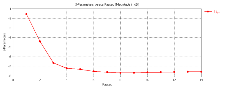
In this example, two adaptation passes are necessary to obtain a suitable result. This means that the maximum deviation of the S-parameters between the first and the second run is less than 2%.
The convergence process
of the input reflection S1,1 during the mesh adaptation can be visualized
by selecting 1D Results ![]() Adaptive Meshing
Adaptive Meshing ![]() S-Parameters
S-Parameters ![]() S1,1 from the navigation tree and select dB scale:
S1,1 from the navigation tree and select dB scale:

You have the option of reducing the accuracy limit for the mesh adaptation or starting the adaptation with a finer starting mesh resolution to obtain even more accurate results. However, these options will certainly increase the simulation time and might be more recommendable after the basic design state of the antenna device is finished. Another possibility for obtaining an impression of the reliability of a solution is to perform a second simulation with a completely different solver and mesh type, as will be shown in the following chapter.
Please note: Refer to the Workflow and Solver Overview manual for more information on using Template Based Postprocessing for automated extraction and visualization of arbitrary results from various simulation runs.
CST MICROWAVE STUDIO offers a variety of frequency domain solvers that are specialized for different types of problems. They differ not only by their algorithms, but also by the type of grid on which they are based. The general purpose frequency domain solvers are available for hexahedral grids as well as tetrahedral grids.
The availability of a frequency domain solver within the same environment offers a very convenient method of cross-checking results produced by the time domain solver with minimal additional effort.
o Making a Copy of Transient Solver Results
Before performing a simulation with a frequency domain solver, you may want to keep the results of the transient solver to allow for an easy comparison of the two simulations. To obtain the copy of the current results: Select, for example, the |S| dB folder in 1D Results, then press Ctrl+c and Ctrl+v. The copy of the result curve will be created in the selected folder. The name of the copy will be S1,1_1. You may rename it to S1,1_TD with the Rename command from the context menu. Use Add new tree folder from the context menu to create an extra folder. Please note that at the current time it is not possible to make a copy of 2D or 3D results.
o Optimize Structure for Tetrahedral Mesh
In the following section, the general purpose frequency domain solver is applied to the tetrahedral mesh. This solver is less efficient if there are PEC sheets with very small, but non zero thicknesses, as represented by the antenna patch in our example. Because this thickness has a rather small influence on the results compared to a zero thickness, we rebuild the patch as a PEC sheet, as shown in the following section.
First, select the patch
in the navigation tree and then select the patch's bottom face using the
face pick tool (Modeling:
Picks ![]() Picks
Picks ![]()
![]() Pick Points,
Edges or Faces). Therefore rotate the structure
as shown in the picture below and double click on the patch.
Pick Points,
Edges or Faces). Therefore rotate the structure
as shown in the picture below and double click on the patch.
A PEC sheet is easily
created from the selected face by applying Modeling:
Shapes ![]() Faces and Apertures
Faces and Apertures ![]()
![]() Shape from Picked Faces:
Shape from Picked Faces:
Enter a suitable name
for the new shape (patch0) and confirm the creation by pressing
the OK button. Finally, delete the old patch (component1 ![]() patch)
so that only the newly created patch with zero height (component1
patch)
so that only the newly created patch with zero height (component1 ![]() patch0)
remains.
patch0)
remains.
There may be old results present from the previous transient solver run that will be overwritten when changing the model. In this case, the following warning message appears:
Press OK to acknowledge deletion of the previous results.
In order to allow a
tetrahedral-based calculation, we change the Mesh type from hexahedral
to tetrahedral in the Mesh Properties dropdown list Home:
Mesh![]() Global Properties
Global Properties
![]() :
:
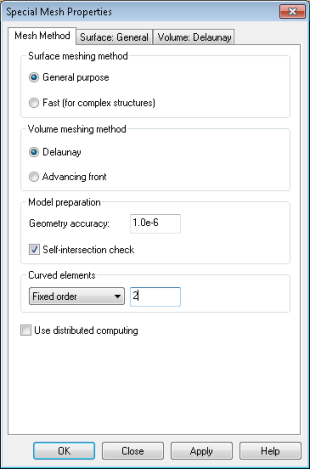
This selection can also be performed directly in the Frequency Domain Solver Parameters dialog box when choosing the desired solver type, as demonstrated in the following chapter. Furthermore, regarding the circular geometry of the patch antenna and its coaxial feed, it is advisable to use curved elements. This ensures an accurate representation of the curved structure.
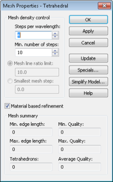
Open the Special Mesh Properties dialog box by pressing the Specials button. On the Mesh Method tab set Curved element as Fixed Order and assign to the parameter the value 2. Otherwise just accept the other default settings. Press the Help button to obtain more information on the settings.
o Frequency Domain Solver Settings
In order to now start
a frequency domain simulation the currently active solver has to be changed
to Home:
Simulation ![]() Start Simulation
Start Simulation ![]() Frequency
Domain Solver
Frequency
Domain Solver
![]() :
:
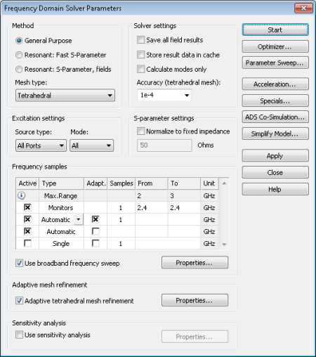
There are three different methods to choose from. For the example here, please choose the General Purpose frequency domain solver. In the Mesh Type combo box you may choose between Hexahedral and Tetrahedral Mesh. Due to the previously made settings in the Mesh Properties dialog box, the Tetrahedral Mesh is already selected.
S-parameters in the frequency domain are obtained by solving the field problem at different frequency samples. These single S-parameter values are then used by the broadband frequency sweep to get the continuous S-parameter values. With the default settings in the Frequency samples frame, the number and position of the frequency samples are chosen automatically in order to fit the required accuracy limit throughout the entire frequency band.
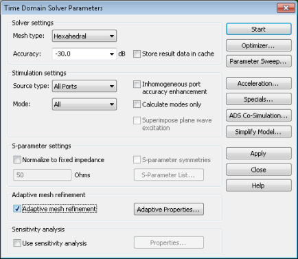
Unlike the time domain solver, the tetrahedral frequency domain solver should always be used with the Adaptive tetrahedral mesh refinement. Otherwise, the initial mesh may lead to a poor accuracy. Therefore, the corresponding check box is activated by default.
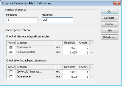
Furthermore, to ensure that the adaptation will satisfy the desired accuracy limit, we increase the Maximum number of passes to 20 in the Adaptive Tetrahedral Mesh Refinement dialog box by pressing the Properties button of the mesh refinement:
After confirming this setting with the OK button, everything is now ready; you may press Start to start the calculation. A progress bar and abort button appear in the status bar, displaying some information about the solver stages. After the desired accuracy for the S-parameter has been reached, the simulation stops. When the simulation has finished or has been aborted, both items disappear again. During the simulation, the Message Window will display details about the performed simulation.
Congratulations, you have simulated the patch antenna using the general purpose tetrahedral frequency domain solver! Lets review the results.
o 1D Results (S-Parameters)
You can visualize the
maximum difference of the S-parameters for two subsequent passes (and
for the specific adaptation frequency) by selecting 1D Results ![]() Adaptive Meshing
Adaptive Meshing
![]() Delta S
from the navigation tree. In the following picture the adaptation for
the 2.4 GHz frequency is shown:
Delta S
from the navigation tree. In the following picture the adaptation for
the 2.4 GHz frequency is shown:
As evident from the above diagram, several passes of the mesh refinement were required to obtain highly accurate results within the given accuracy level that is set to 1% by default.
As for the transient
solver run, you can view the S-parameters by selecting 1D Results ![]() S-Parameters
in the navigation tree and selecting 1D Plot:
Plot Type
S-Parameters
in the navigation tree and selecting 1D Plot:
Plot Type ![]() dB
dB ![]() for dB representation.
for dB representation.
It is possible to precisely
determine the operational frequency for the patch antenna. Activate the
axis marker by pressing 1D Plot:
Markers
![]() Axis
Marker
Axis
Marker ![]() . Now you can move the marker to the S11 minimum and pinpoint
a resonance frequency for the patch antenna of about 2.4 GHz.
. Now you can move the marker to the S11 minimum and pinpoint
a resonance frequency for the patch antenna of about 2.4 GHz.
o 2D and 3D Results (Port Modes and Farfield Monitors)
Finally, you can observe
the 2D and 3D field results. You should first inspect the port modes that
can be easily displayed by opening the 2D/3D Results ![]() Port
Modes
Port
Modes ![]() Port1 folder from the navigation tree. To visualize the
electric field of the port mode, please click on the e1 folder.
Open the Select Port Mode dialog box by selecting Results
Port1 folder from the navigation tree. To visualize the
electric field of the port mode, please click on the e1 folder.
Open the Select Port Mode dialog box by selecting Results ![]() Select Mode
Frequency from the main menu and ensure that the frequency is 2.4
GHz. Please confirm your setting by pressing OK.
After properly rotating the view and tuning some settings in the plot
properties dialog box, you should obtain a plot similar to the following
picture (please refer to the Workflow and Solver Overview manual for more information on how to change the plots parameters):
Select Mode
Frequency from the main menu and ensure that the frequency is 2.4
GHz. Please confirm your setting by pressing OK.
After properly rotating the view and tuning some settings in the plot
properties dialog box, you should obtain a plot similar to the following
picture (please refer to the Workflow and Solver Overview manual for more information on how to change the plots parameters):
The plot also shows some important properties of the mode such as mode type, propagation constant and line impedance. The port mode at the second port can be visualized in the same manner.
In addition to the resonance frequency, the farfield is another important parameter in antenna design.
The farfield solution
of the antenna device can be shown by selecting the corresponding monitor
entry in the Farfields folder from the navigation tree. For example,
the farfield at the frequency 2.4 GHz can be visualized by clicking on
the Farfields ![]() farfield (f=2.4)
[1] entry, showing the directivity over the phi and theta angle (the
plot settings such as color ramp can be accessed selecting FarField Plot:
Plot Properties
farfield (f=2.4)
[1] entry, showing the directivity over the phi and theta angle (the
plot settings such as color ramp can be accessed selecting FarField Plot:
Plot Properties![]() Properties
Properties
![]() )
)
Please note: You have the option of changing the FarField Plot:
Plot Properties![]() Properties
Properties ![]() angle step to 5 degrees for a better
angle accuracy of the plot.
angle step to 5 degrees for a better
angle accuracy of the plot.
You can see that the maximum power is radiated in the positive z-direction. Note that there are several other options available to plot a farfield: the Polar plot, the Cartesian plot and the 2D plot.
o Comparing the results
The following figure shows the comparison between the S-parameter result of the transient hexahedral and the frequency domain tetrahedral simulations:
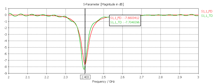
Obviously, the result curves are quite similar to each other; they are not, however, precisely identical. When comparing two completely different numerical methods, you should keep in mind that transient analysis is based on a hexahedral grid and frequency domain analysis is based on tetrahedral grid. Consequently, the results show some differences in detail but the same overall qualitative behavior and therefore provide a satisfying validation. The differences are due to dispersion effects and this example is especially affected by the circular-shaped structural elements. Here, for example, the starting mesh resolution of the tetrahedral grid strongly influences the final accuracy of the simulation. If more accurate results are needed, both simulations can be calculated with a finer starting mesh resolution that would lead to a better convergence.
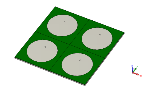
Starting from the single patch antenna constructed in this chapter, the extension to a four element antenna array will now be demonstrated. Here, we will concentrate purely on the farfield calculations. All other results can be analyzed in a manner similar to the first part of this tutorial.
Please note that all following steps are performed using the transient solver. The procedure, however, can be applied to the frequency domain solver and its farfield results presented in the previous chapter.
The array calculation will be done in three steps: First, the antenna array feature is applied to the farfield results of the single patch antenna. Afterwards, the structure is physically expanded to the 2x2 antenna array and we use a result combination of a sequential excitation as well as a simultaneous excitation to obtain the radiation characteristics.
Starting from the farfield results of the simulated single patch antenna, it is possible to calculate the farfield distribution for an arbitrary antenna array consisting of identical antenna elements as a post-processing step.
Later, we will expand the antenna example by constructing a
2x2 antenna array pattern, so it is preferable to apply the mentioned
array calculation feature to the same rectangular array dimension. Click
on the Farfields ![]() farfield (f=2.4) [1] entry in the navigation tree and
open the corresponding dialog box by pressing FarField Plot:
Plot Properties
farfield (f=2.4) [1] entry in the navigation tree and
open the corresponding dialog box by pressing FarField Plot:
Plot Properties![]() Properties
Properties
![]() , then the
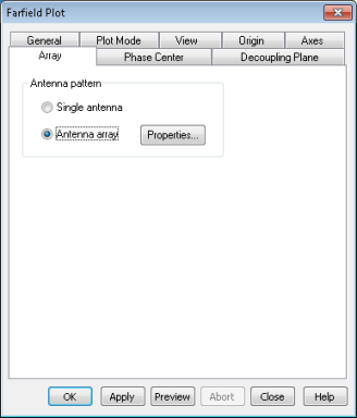
tab Array and selecting the radio button Antenna array.
, then the
tab Array and selecting the radio button Antenna array.
Afterwards, select Properties and insert the values to create the rectangular 2x2 array pattern in the XY-plane with a spatial shift of 60 mm (due to the dimension of the antenna substrate) and a phase shift of +90 degrees:
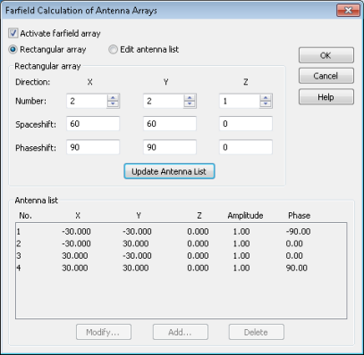
By pressing the Update Antenna List button, you can display the coordinates and their respective amplitudes and phase values in the Antenna list, as seen in the above dialog box.
Please note: The Antenna list can be modified if the radio button Edit antenna list is activated. This means that not only rectangular arrays with constant space and phase shift can be calculated, but by adding and modifying single antennas any array pattern with arbitrary amplitude and phase values can be defined.
Please confirm with the OK button to calculate the resulting farfield of the defined array pattern. The following screenshot demonstrates that the array arrangement together with the constant phase shift of +90 degrees produce not only a constructive superposition with an increased directivity, but also a slight rotation of the main loop in negative x and y directions:

Please note: You have the option of changing
the FarField Plot:
Plot Properties![]() Properties
Properties ![]() angle step to 5 degrees for a better
angle accuracy of the plot.
angle step to 5 degrees for a better
angle accuracy of the plot.
Please feel free to define some more array patterns to analyze the resulting changes in the farfield distribution. Here, you have a fast and efficient way to design various antenna arrays without necessitating the restart of a calculation.
Regarding the following
calculations: the antenna array feature should now be disabled; therefore,
please reset the Antenna Array selection in the Farfield Plot dialog box FarField Plot:
Plot Properties![]() Properties
Properties ![]() back to Single antenna.
back to Single antenna.
The construction of the array is based on the translation feature for selected objects that will be applied to the complete component of the single patch antenna. This procedure is also applicable to single objects or an arbitrary multiple selection of objects, even when selected from different components.
Before you start, please
switch off the local coordinate system, if necessary, by clicking Modeling:
WCS![]() Local WCS
Local WCS
![]()
Now, please select
component1 from the Components folder in the navigation
tree and perform a transformation of the complete component (press the
toolbar icon Modeling:
Tools ![]() Transform
Transform ![]() Translate
Translate
![]() ). Choose the
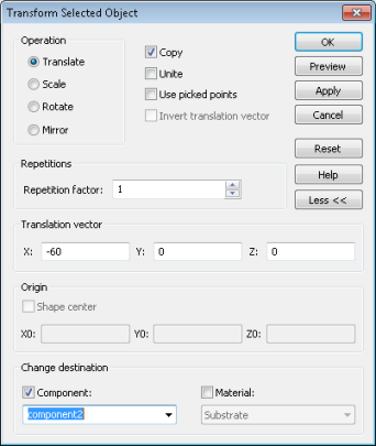
Translate function in the upcoming Transform Selected Object dialog
box and enter the value of -60 (referring to the previously defined units
of mm) for the x-component of the translation vector, corresponding to
the structural dimension.
). Choose the
Translate function in the upcoming Transform Selected Object dialog
box and enter the value of -60 (referring to the previously defined units
of mm) for the x-component of the translation vector, corresponding to
the structural dimension.
In order to gather all translated shapes as a new component, please activate the Copy and Component check boxes and then select [New Component] from the Component dropdown menu (it could be necessary to click on the More button) to create the destination group component2.
Finally, perform the translation operation with the OK button:
Because the structure will change when this operation is performed, you will be informed that the previously calculated results need to be deleted. Confirm this message by clicking OK.
Now, CST MICROWAVE STUDIO copies the selected component to the coordinates of its translated position and creates a new component, containing all translated single shapes of the patch antenna.
The resulting structure, consisting of two identical patch antennas, will then look as follows:

Please repeat the described transformation in the negative y-direction for both components (component1 and component2), again with a space shift of 60 mm. The occurring intersection dialog box can be solved by activating the None button, so that the final array pattern will be created as follows:
To complete the model, the remaining ports of the newly created patch antennas must be created. This is carried out in a similar manner to the definition of the first port by picking the corresponding port area (the bottom face of the respective substrate cylinders) and defining a port, again with only one mode.
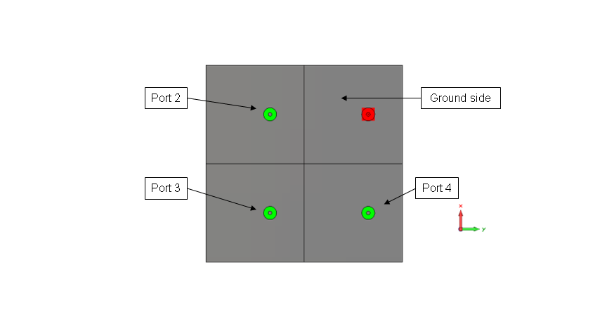
In order to receive farfield results where all patches are driven simultaneously, the results are combined in a post-processing step. This means that, at first, each port is excited individually one after another, after which arbitrary combinations of these excitations can be defined with respect to different amplitude and phase values.
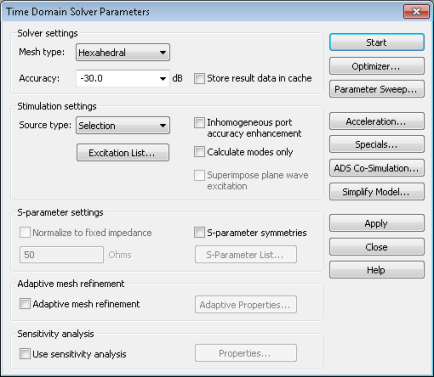
o Define the Solvers Parameters and Start the Calculation
As described earlier,
the solvers parameters are specified in the Transient Solver Parameters
dialog box that can be opened by selecting Home:
Simulation
![]() Start Simulation
Start Simulation ![]() Time Domain Solver
Time Domain Solver ![]() .
.
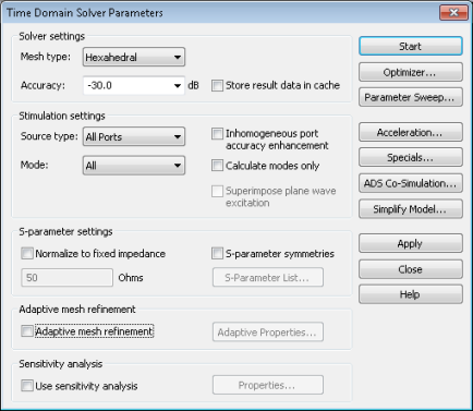
Because all ports should be calculated, you must be certain that All Ports is selected in the Source type dropdown list. The Adaptive mesh refinement check box must also be deactivated. Now you can press the Start button to run the calculation. Again, the progress bar appears indicating, in addition to the calculations status, the current solver cycle.
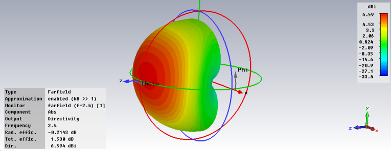
After the transient
solver has finished, please observe the farfield of a single patch from
the array. It appears quite similar to the farfield distribution of the
previously calculated single patch antenna. The following screenshot shows
the directivity over the angles theta and phi. Click on the Farfields
![]() farfield (f=2.4)
[1] folder in the navigation tree to bring your plot into view:
farfield (f=2.4)
[1] folder in the navigation tree to bring your plot into view:
o Combine Results
The most interesting
results, however, are those where all patches are driven at one time with
a pre-determined amplitude and phase variation being taken into account.
This can be produced by CST MICROWAVE STUDIO using the Combine
results option. Press Post Processing:
Combine Results
![]() to bring the Combine Calculation Results
window into view.
to bring the Combine Calculation Results
window into view.
Now you have the option of changing the amplitude and phase excitation in the port mode list. In order to compare the farfield result with the previously demonstrated antenna array feature, we define identical antenna settings, i.e. the first antenna receives a phase shift of +90 degrees, the third antenna of -90 degrees and the two remaining antennas 0 degrees:

Please note: The corresponding monitor label will be generated automatically due to the settings of the port mode combination; however, by disabling the Automatic labeling button you are able to enter a label of your choice.
After confirming your settings with the Combine button, you will observe a new farfield subfolder farfield (f=2.4) [1[1,90]+2[1,0]+3[1,-90]+4[1,0]] in the navigation tree. By clicking on it you will display the following farfield distribution that is quite similar to the result of the antenna array feature:
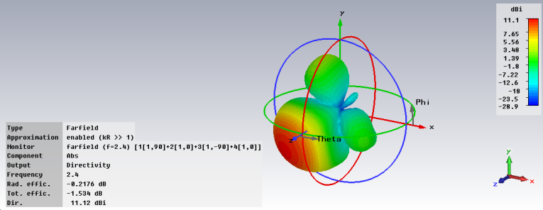
As you can see, the combination of results is time efficient because you do not have to restart the solver; just enter the amplitude and phase and view the combined generated farfield plot.
Another possibility for obtaining the farfield result of the array pattern is the excitation of all four ports simultaneously. In contrast to the combine result facility, here only one transient solver run is required. However, the phase shift relationship between the antenna elements has to be known before the solver is started.
Please note: The definition of a phase shift in connection with a simultaneous excitation of different ports will be converted, using the defined reference frequency, into a constant time shift between the port excitation signals. Therefore, in order to examine a farfield result, the reference frequency must be identical to the frequency of the farfield monitor.
In order to define
the simultaneous excitation you must choose Selection in the Source
type dropdown list in the Transient Solver Parameters dialog box (selecting
Home:
Simulation
![]() Start Simulation
Start Simulation ![]() Time Domain Solver
Time Domain Solver ![]() ):
):
Pressing the Excitation List button opens the following dialog box, where the selective and simultaneous port excitation settings can be defined:
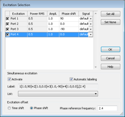
Since all four existing ports will be excited, please activate all available check buttons in the port mode list. In order to enter the amplitude and phase values, you must first activate the Simultaneous excitation by checking the corresponding Activate button. Please activate the Phase shift check box and enter a reference frequency of 2.4 GHz so that the result will be compatible to the combined farfield monitor in the previous chapter. Again, all antennas are driven with an amplitude value of one and phase values of 90, 0, -90, 0 degrees. Please double-check your settings against the dialog box above and confirm with the OK button.
Finally, you can press
the Start button in the Transient Solver Parameters dialog box
(selecting Home:
Simulation
![]() Start Simulation
Start Simulation ![]() Time Domain Solver
Time Domain Solver ![]() ) to start the simultaneous calculation.
Again, the progress bar appears indicating, in addition to the calculations
status, the simultaneous solver calculation.
) to start the simultaneous calculation.
Again, the progress bar appears indicating, in addition to the calculations
status, the simultaneous solver calculation.
Observe the input time
signals (after the calculation has finished, you can select specific curves
in your 1D plot view by choosing Port Signals ![]() Select Curves
to open the corresponding dialog box). In the picture below you can
see the time delay of the different input signals due to the defined phase
shifts of the ports:
Select Curves
to open the corresponding dialog box). In the picture below you can
see the time delay of the different input signals due to the defined phase
shifts of the ports:

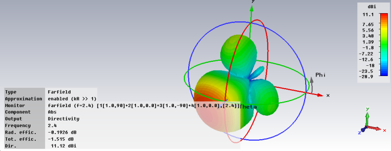
After the transient solver
has finished, you will find the resulting farfield information in the
Farfields ![]() farfield (f=2.4) [1[1.0,90]+2[1.0,0.0]+3[1.0,-90.0]+4[1.0,0.0],[2.4]]
folder. Clicking on it will show the following farfield plot of the directivity
over the angles theta and phi. As expected, the result is very similar
to that produced by combining the results of the four single port excitations
in the previous chapter:
farfield (f=2.4) [1[1.0,90]+2[1.0,0.0]+3[1.0,-90.0]+4[1.0,0.0],[2.4]]
folder. Clicking on it will show the following farfield plot of the directivity
over the angles theta and phi. As expected, the result is very similar
to that produced by combining the results of the four single port excitations
in the previous chapter:
Please note: If some ports are stimulated simultaneously the magnitude and phase of the normalized signal spectrum at the ports are recorded (F-Parameters) as well as so-called active S-Parameters for the excited ports.
Congratulations! You have just completed the antenna tutorial that should have provided you with a good working knowledge on how to use CST MICROWAVE STUDIO to calculate S-parameters and farfield results. The following topics have been covered:
1. General modeling considerations, using templates, etc.
2. Model a planar structure by using the extrude tool, creating the substrate, circular patch antenna and a coaxial feed.
3. Define waveguide ports.
4. Define frequency range.
5. Define farfield monitors.
6. Start the transient or the frequency domain solver.
7. Visualize port signals and S-parameters.
8. Visualize port modes and farfield results.
9. Obtain accurate and converged results using the mesh adaptation.
10. Check the truncation error of the time signals.
11. Application of the antenna array feature.
12. Extend the single patch antenna to a four element antenna array and combine single calculation results as well as perform a simultaneous excitation.
You can obtain more information for each particular step from the online help system that can be activated either by pressing the Help button in each dialog box or by pressing the F1 key at any time to obtain context sensitive information.
In some cases we have referred to the Workflow and Solver Overview manual that is also a good source of information for general topics.
In addition to this tutorial, you can find more S-parameter calculation examples for planar structures or various antenna models in the Examples folder in your installation directory. Each of these examples contains a Readme item in the navigation tree that provides more information about the particular device.
Finally, you should refer to the Online documentation for more in-depth information on issues such as the fundamental principles of the simulation method, mesh generation, usage of macros to automate common tasks, etc.
And last but not least: Please visit one of the training classes held regularly at a location near you. Thank you for using CST MICROWAVE STUDIO!


HFSSЪгЦЕНЬГЬ ADSЪгЦЕНЬГЬ CSTЪгЦЕНЬГЬ Ansoft Designer жаЮФНЬГЬ
|
Copyright © 2006 - 2013 ЮЂВЈEDAЭј, All Rights Reserved вЕЮёСЊЯЕЃКmweda@163.com |
|