![]()
![]()
|
Transient Solver: |
|
|
Frequency Domain Solver Tetrahedral: |
|
Geometric Construction and Solver Settings
Introduction and Model Dimensions
S-Parameter and Field Calculation
Comparison of the Solver Results
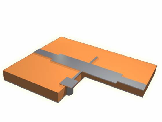
In this tutorial you will learn how to simulate planar devices. As a typical example for a planar device, you will analyze a Microstrip Phase Bridge. The following explanations on how to model and analyze this device can be applied to other planar devices, as well.
CST MICROWAVE STUDIO can provide a wide variety of results. This tutorial, however, concentrates solely on the S-Parameters and surface currents.
We strongly suggest that you carefully read through the CST STUDIO SUITE Getting Started and CST MICROWAVE STUDIO Workflow and Solver Overview manual before starting this tutorial.

All dimensions are given in milli-inches (mil). The thickness of the metallization is 0.118 mil.
The structure depicted above consists of two different materials: The aluminum oxide substrate (Al2O3) and the stripline metallization. There is no need to model the ground plane since it can easily be described using a perfect electric boundary condition.
This tutorial will take you step by step through the construction of your model, and relevant screen shots will be provided so that you can double-check your entries along the way.
o Create a New Project
After launching the CST STUDIO SUITE
you will enter the start screen showing you a list of recently opened
projects and allowing you to specify the application which suits your
requirements best. The easiest way to get started is to configure a project
template which defines the basic settings that are meaningful for your
typical application. Therefore click on the Create
Project button ![]() in the New Project section.
in the New Project section.
Next you should choose the application area, which is Microwaves & RF for the example in this tutorial and then select the workflow by double-clicking on the corresponding entry.

For the Planar Device structure, please
select Circuits
& Components ![]() Planar Filters
Planar Filters
![]() Time Domain Solver
Time Domain Solver ![]() .
.
At last you are requested to select the units which fit your application best. For the Planar Device structure, please select the dimensions as follows:
|
Dimensions: |
mil |
|
Frequency: |
GHz |
|
Time: |
ns |
For the specific application in this tutorial the other settings can be left unchanged. After clicking the Next button, you can give the project template a name and review a summary of your initial settings:
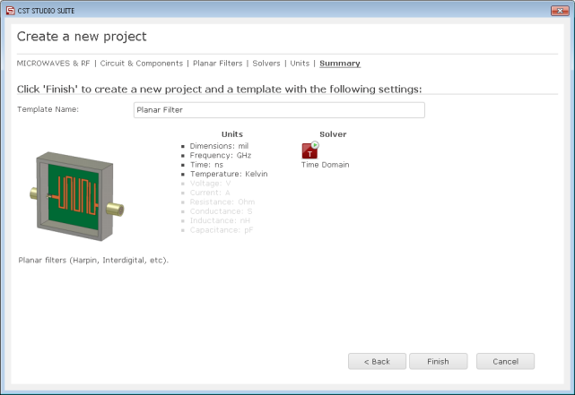
Finally click the Finish button to save the project template and to create a new project with appropriate settings. CST MICROWAVE STUDIO will be launched automatically due to the choice of the application area Microwaves & RF.
Please note: When you click again on the File: New and Recent you will see that the recently defined template appears below the Project Templates section. For further projects in the same application area you can simply click on this template entry to launch CST MICROWAVE STUDIO with useful basic settings. It is not necessary to define a new template each time. You are now able to start the software with reasonable initial settings quickly with just one click on the corresponding template.
Please
note: All settings made for a project template can be modified
later on during the construction of your model. For example, the units
can be modified in the units dialog box (Home:Settings ![]() Units
Units ![]() ) and the solver type can be selected
in the Home:Simulation
) and the solver type can be selected
in the Home:Simulation ![]() Start Simulation drop-down
list.
Start Simulation drop-down
list.
o Set the Working Planes Properties
The next step is usually to set the
working plane properties to make the drawing plane large enough for your
device. Because the structure has a maximum extension of 300 mil
along a coordinate direction, the working plane size should be set to
at least 400 mil. These settings can be changed in a dialog box
that opens after selecting View:Visibility ![]() Working Plane
Working Plane ![]()
![]() Working Plane
Properties. Please note that we will
use the same document conventions here as introduced in the Workflow and Solver Overview manual.
Working Plane
Properties. Please note that we will
use the same document conventions here as introduced in the Workflow and Solver Overview manual.
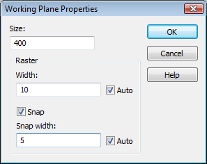
In this dialog box, you should set the Size to 400 (the unit that has previously been set to mil is displayed in the status bar), the Raster width to 10 and the Snap width to 5 to obtain a reasonably spaced grid. Please confirm these settings by pressing the OK button.
o Draw the Substrate Brick
The first construction step for modeling
a planar structure is usually to define the substrate layer. This
can be easily achieved by creating a brick made of the substrates material.
Please activate the brick creation mode Modeling:
Shapes ![]() Brick
Brick ![]() .
.
When you are prompted to define the first point, you can enter the coordinates numerically by pressing the Tab key that will open the following dialog box:
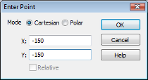
In this example, you should enter a substrate block that has an extension of 300 mil in each of the transversal directions. The transversal coordinates can thus be described by X = -150, Y = -150 for the first corner and X = 150, Y = 150 for the opposite corner, assuming that the brick is modeled symmetrically to the origin. Please enter the first points coordinates X = -150 and Y = -150 in the dialog box and press the OK button.
You can repeat these steps for the second point:
1. Press the Tab key
2. Enter X = 150, Y = 150 in the dialog box and press OK.
Now you will be requested to enter the height of the brick. This can also be numerically specified by pressing the Tab key again, entering the Height of 25 and pressing the OK button. Now the following dialog box will appear showing you a summary of your previous input:

Please check all these settings carefully. If you encounter any mistake, please change the value in the corresponding entry field.
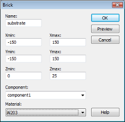
You should now assign a meaningful name to the brick by entering e.g. substrate in the Name field. Since the brick is the first object you have modeled thus far, you can keep the default settings for the first Component (component1).
Please note: The use of different components allows you to combine several solids into specific groups, independent of their material behavior. However, in this tutorial it is convenient to construct the complete microstrip device as a representation of one component.
The Material setting of the brick must be changed to the desired substrate material. Because no material has yet been defined for the substrate, you should open the layer definition dialog box by selecting [New Material...] from the Material dropdown list:
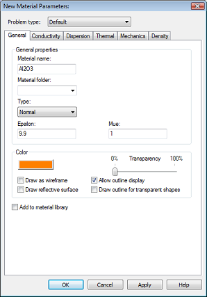
In this dialog box you should define a new Material name (e.g. Al2O3) and set the Type to a Normal dielectric material. Afterwards, specify the material properties in the Epsilon and Mue fields. Here, you only need to change the dielectric constant Epsilon to 9.9. Finally, choose a color for the material by clicking the color field. Your dialog box should now look similar to the picture above before you press the OK button.
Please note:
The defined material Al2O3 will now be available inside the current project
for the creation of other solids. However, if you also want to save
this specific material definition for other projects, you may check the
button Add to material library. You will have access to this
material database by clicking on Load from Material Library in
the Materials context menu in the navigation tree.
In addition, the dialog box allows you to define different material folders. Therefore click on the Materials drop down box and enter an according name. For simplicity we keep the box empty, the material will then appear in the top layer of the Materials folder in the navigation tree.
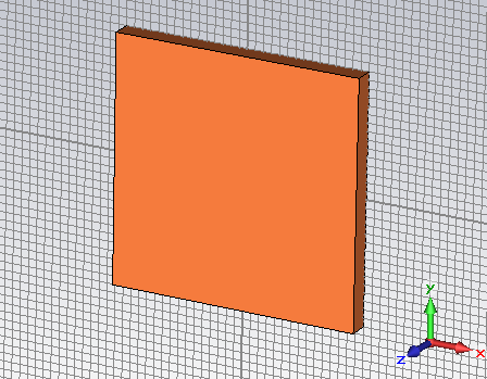
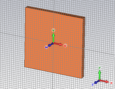
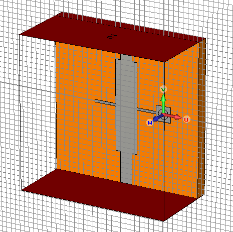
Back in the brick creation dialog box you can also press the OK button to finally create the substrate brick. Your screen should now look as follows (you can press the Space key in order to zoom the structure to the maximum possible extent):
o Model the Stripline Metallization
The next step is to model the stripline
metallization on top of the substrate. Therefore, you should first
move the drawing plane on top of the substrate. This can be easily
achieved by activating the face pick tool Modeling:
Picks ![]() Picks
Picks ![]()
![]() Pick Points,
Edges or Faces and double-clicking on the substrates
top face (upper face in z direction). The face selection should
then be visualized as in the following picture:
Pick Points,
Edges or Faces and double-clicking on the substrates
top face (upper face in z direction). The face selection should
then be visualized as in the following picture:
After the face has been selected, you
can align the working coordinate system with its plane. Therefore,
please either select Modeling:
WCS
![]() Align WCS
Align WCS
![]() , or simply use the shortcut w.
Now the drawing plane will be aligned with the top of the substrate:
, or simply use the shortcut w.
Now the drawing plane will be aligned with the top of the substrate:
The easiest way to draw the metallization
is to use a polygonal extrusion. This tool can be entered by selecting
Modeling:
Shapes ![]() Extrude
Extrude ![]() . After the polygonal extrude mode is
active, you are requested to enter the polygons points. For each
of these points you should press the Tab key and enter the point
coordinates manually according to the following table (you may either
enter the expressions or the absolute values given in brackets):
. After the polygonal extrude mode is
active, you are requested to enter the polygons points. For each
of these points you should press the Tab key and enter the point
coordinates manually according to the following table (you may either
enter the expressions or the absolute values given in brackets):
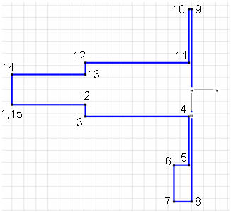
|
Point |
U coordinate |
V coordinate |
|
1 |
25 / 2 (=12.5) |
-150 |
|
2 |
25 / 2 (=12.5) |
-177.58 / 2 (= -88.79) |
|
3 |
44.41 / 2 (=22.205) |
-177.58 / 2 (= -88.79) |
|
4 |
44.41 / 2 (=22.205) |
-4.9 / 2 (= -2.45) |
|
5 |
44.41 / 2 + 40.4 (=62.605) |
-4.9 / 2 (= -2.45) |
|
6 |
44.41 / 2 + 40.4 (=62.605) |
-30 / 2 (= -15) |
|
7 |
44.41 / 2 + 40.4 + 30 (=92.605) |
-30 / 2 (= -15) |
|
8 |
44.41 / 2 + 40.4 + 30 (=92.605) |
0 |
|
9 |
-44.41 / 2 - 44.68 (= -66.885) |
0 |
|
10 |
-44.41 / 2 - 44.68 (= -66.885) |
-4.9 / 2 (= -2.45) |
|
11 |
-44.41 / 2 (= -22.205) |
-4.9 / 2 (= -2.45) |
|
12 |
-44.41 / 2 (= -22.205) |
-177.58 / 2 (= -88.79) |
|
13 |
-25 / 2 (= -12.5) |
-177.58 / 2 (= -88.79) |
|
14 |
-25 / 2 (= -12.5) |
-150 |
|
15 |
25 / 2 (=12.5) |
-150 |
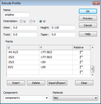
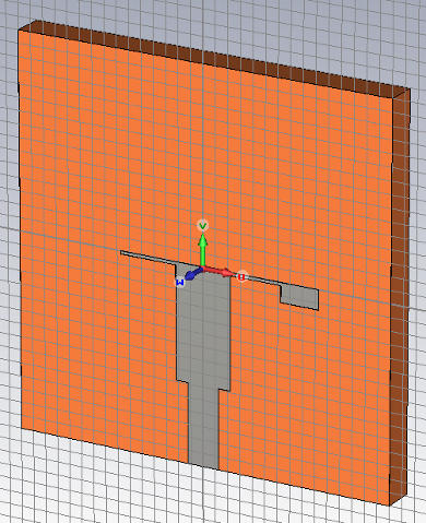
Please note that we do not recommend entering the points relative to each other here because this would make the detection of mistakes during the coordinate input more difficult. After you have entered the last point from the table that closes the polygon, the extrusion tool requests you to enter the height. Please press the Tab key again and enter the Height as 0.118 and press OK. Afterwards, your screen should look similar to:
If your polygon does not look like the one in the picture above, please double-check your input in the dialogs point list. Afterwards, please assign a Name to the solid (e.g. stripline) and change the Material assignment to be a perfect electrical conductor (PEC).
After finally pressing the OK button, the structure should look as follows:
To this point, you have modeled half
of the stripline structure. The other half can be created by mirroring
the structure at the UW plane of the working coordinate system.
Please select the stripline by double-clicking on it (the substrate will
then become transparent) and then open the transform dialog box Modeling:
Tools ![]() Transform
Transform ![]() Translate
Translate
![]() :
:
![]()
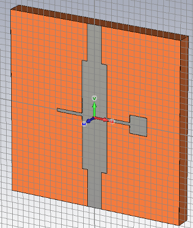
In this dialog box you should change the Operation to Mirror before you set the V-coordinate of the Mirror plane normal to 1. Afterwards, please switch on the Copy as well as the Unite option to copy the existing shape before mirroring it and to unite the original shape with the mirrored copy. You may check your settings using the Preview button. Finally, press OK to create the full stripline. Your model should then look as follows:
o Model the Via
After successfully modeling the stripline structure, the next step is to model the via that should be located in the center of the square pad. The alignment between these two geometric elements can be specified by moving the working coordinate system to the center of the pad.
Please activate the pick tool Modeling:
Picks ![]() Picks
Picks ![]()
![]() Pick Points,
Edges or Faces and double-click on one of the
corners of the pad. Repeat the same steps in order to pick the point
from the opposite corner, as well. The picture below shows an example
of how your structure should now appear:
Pick Points,
Edges or Faces and double-click on one of the
corners of the pad. Repeat the same steps in order to pick the point
from the opposite corner, as well. The picture below shows an example
of how your structure should now appear:
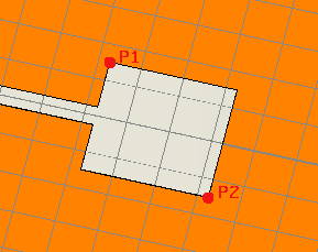
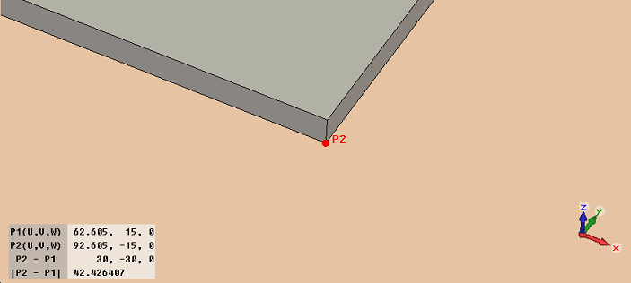
Please note: Due to the small thickness it may be difficult to pick the appropriate points on the drawing plane because they are very close to the points from the metallizations top face. Please zoom into the two edges until you can verify that the correct points are picked. Finally for pick point 2, situation should look as follows:
If you have made a mistake, please clear
all picked points Modeling:
Picks
![]() Clear Picks
Clear Picks
![]() and try again. The next step is to replace both points
by a point in the middle of both. This can be easily achieved by
invoking the command Modeling:
Picks
and try again. The next step is to replace both points
by a point in the middle of both. This can be easily achieved by
invoking the command Modeling:
Picks
![]() Pick Point
Pick Point ![]()
![]() Mean Last Two Points. Now a single point should be selected in the middle
of the pad.
Mean Last Two Points. Now a single point should be selected in the middle
of the pad.
Now the working coordinate system can
be aligned with this point by selecting Modeling:
WCS
![]() Align WCS
Align WCS ![]()
![]() Align WCS
with Selected Point. Your structure
should then look like the following picture:
Align WCS
with Selected Point. Your structure
should then look like the following picture:

The via can now be created using the
cylinder tool: Modeling:
Shapes ![]() Cylinder
Cylinder ![]() . Once the cylinder creation mode is active you
are requested to pick the center of the cylinder. Because this is
now the origin of the working coordinate system, you can simply press
Shift+Tab to open the dialog box for numerically entering the coordinates
and confirm the settings by pressing OK (please note that holding
down the Shift key while pressing the Tab key opens the
dialog box with the coordinate values initially set to zero rather than
to the current mouse pointers location).
. Once the cylinder creation mode is active you
are requested to pick the center of the cylinder. Because this is
now the origin of the working coordinate system, you can simply press
Shift+Tab to open the dialog box for numerically entering the coordinates
and confirm the settings by pressing OK (please note that holding
down the Shift key while pressing the Tab key opens the
dialog box with the coordinate values initially set to zero rather than
to the current mouse pointers location).
You are now requested to enter the outer radius of the via. Please press the Tab key again and set the Radius to 10 before pressing the OK button. The Height of the cylinder can then be set to -25 in the same manner. Please skip the definition of the inner radius by pressing the Esc key (the via should be modeled as solid cylinder here) and check your settings in the following dialog box:
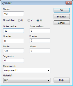
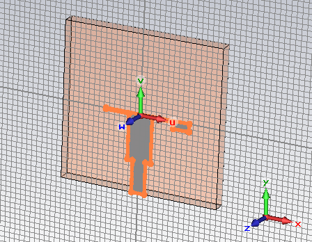
Finally set the Name of the cylinder to "via" and the Material assignment to PEC and press the OK button. The model should then finally look as follows (please use Ctrl+w to toggle the wireframe visualization mode on and off):

o Add Space on Top of the Stripline
Since the structure will be embedded in a perfect electrically conducting box, some space is needed between the metallization layer and the top wall of the enclosure.
This can be easily achieved in the Background
Properties dialog box that can be opened by selecting Modeling:
Materials ![]() Background
Background ![]() .
.
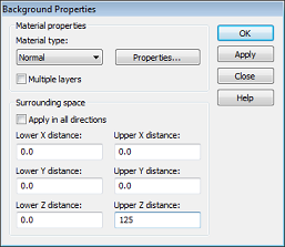
In most cases it is sufficient to add an additional space of about five times the height of the substrate on top of the metallization. Thus, you should now enter 125 (= 5 * 25) in the Upper Z distance field and press OK.
o Define Ports
The next step is to add the ports to the microstrip device for which the S-Parameters will later be calculated. Each port will simulate an infinitely long waveguide (here stripline) structure that is connected to the structure at the ports plane. Waveguide ports are the most accurate way to calculate the S-Parameters of microstrip devices and should thus be used here.
A waveguide port extends the structure to infinity. Its transversal extension must be large enough to sufficiently cover the microstrip mode. On the other hand, it should not be chosen excessively large in order to avoid higher order mode propagation in the port. A good choice for the width of the port is roughly ten times the width of the stripline. A proper height is about five times the height of the substrate.
Applying these guidelines to the example here, you find that the optimum ports width is roughly 250 mil and that its height should be about 125 mil. In this example, the whole model has a width of 300 mil and a height of 150 mil. Because these dimensions are close to the optimal port size you can simply take these dimensions and apply the port to the full extension of the model. Read the Workflow and Solver Overview manual to obtain more information on defining waveguide ports.
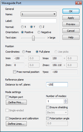
Please open the waveguide port dialog
box Simulation:
Sources
and Loads ![]() Waveguide Port
Waveguide Port ![]() to define the first port. Here, you should
set the Normal of the ports plane to the Y-direction and
its Orientation in the positive Y-direction (Positive).
Because the port should extend across the entire boundary of the model,
you can simply keep the Full plane setting for the transversal
position. Without the Free normal position check button activated,
the port will be allocated as default on the boundary of the calculation
domain.
to define the first port. Here, you should
set the Normal of the ports plane to the Y-direction and
its Orientation in the positive Y-direction (Positive).
Because the port should extend across the entire boundary of the model,
you can simply keep the Full plane setting for the transversal
position. Without the Free normal position check button activated,
the port will be allocated as default on the boundary of the calculation
domain.
The next step is to choose how many modes should be considered by the port. For microstrip devices, a single mode usually propagates along the line. Therefore, you should keep the default setting of one mode.
Lets assume that you are interested in the additional phase shift of the device compared to a microstrip line of the same length. In this case, you could move the phase reference plane for both ports to the center of the structure as shown below:
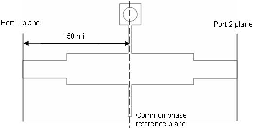
Therefore, please enter the distance between the ports plane and the phase reference plane in the Dist. to ref. plane field. Please note that you must enter a negative number (-150) to move the reference plane inwards. After entering the distance, you may press the Tab key to move the focus to the next dialog element. After a reference plane distance has been set, the location of this plane will be visualized in the main view.
Please finally check the settings in the dialog box and press the OK button to create the port:
You can now repeat the same steps for the definition of the opposite port 2:
1.
Open the waveguide port dialog box Simulation:
Sources
and Loads ![]() Waveguide Port
Waveguide Port ![]()
2. Set the Normal to Y.
3. Set the Orientation to Negative.
4. Enter the reference plane distance of -150.
5. Press OK to store the ports settings.
Your model should now look as follows:
o Define the Boundary Conditions
In this case, the structure is embedded
within a perfect electrically conducting enclosure. Because this
is the default of the CST MICROWAVE STUDIO module ![]() , you do not need to change any settings
here.
, you do not need to change any settings
here.
o Define the Frequency Range
The frequency range for the simulation should be chosen with care. In contrast to frequency domain tools, the performance of a transient solver can be degraded if the chosen frequency range is too small (the opposite is usually true for frequency domain solvers).
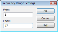
We recommend using reasonably large bandwidths of 20% to 100% for the transient simulation. In this example, the S-Parameters are to be calculated for a frequency range between 6 and 17 GHz. With the center frequency being 11.5 GHz, the bandwidth (17 GHz - 6 GHz = 11 GHz) is about 96% of the center frequency, which is sufficiently large. Thus, you can simply choose the frequency range as desired between 6 and 17 GHz.
Please note: Assuming that you were interested primarily in a frequency range of e.g. 11.5 to 12.5 GHz (for a narrow band filter), then the bandwidth would only be about 8.3%. In this case, it would make sense to increase the frequency range (without losing accuracy) to a bandwidth of 30% that corresponds to a frequency range of 10.2 to 13.8 GHz. This extension of the frequency range could speed up your simulation by more than a factor of three!
In contrast to frequency domain solvers, the lower frequency can be set to zero without any problems! The calculation time can often be reduced by half if the lower frequency is set to zero rather than e.g. to 0.01 GHz.
After the proper frequency band for
this device has been chosen, you can simply open the frequency range dialog
box Simulation:
Settings
![]() Frequency
Frequency
![]() and enter the range from 6 to 17 (GHz) before pressing the OK button
(the frequency unit has previously been set to GHz and is displayed in
the status bar):
and enter the range from 6 to 17 (GHz) before pressing the OK button
(the frequency unit has previously been set to GHz and is displayed in
the status bar):
o Define Monitors for the Surface Current
In addition to the S-Parameters, an interesting result for microstrip devices is the current distribution as a function of frequency. The transient solver in CST MICROWAVE STUDIO is able to obtain the surface current distribution for an arbitrary number of frequency samples from a single calculation run. You can define field monitors to specify the frequencies at which the field data shall be stored.
Please open the monitor definition dialog
box by selecting Simulation:
Monitors
![]() Field Monitor
Field Monitor
![]() :
:
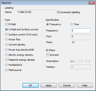
In this dialog box you should select
the Type H-Field ![]() Surface current before you specify the frequency for
this monitor in the Frequency field. Afterwards, you should
press the Apply button to store the monitors data. Please
define monitors for the following frequencies: 6, 9, 12, 15 (with GHz
being the currently active frequency unit). Please make sure that
you press the Apply button for each monitor. The monitor
definition is then added in the Monitors folder in the navigation
tree. The volume in which the fields are recorded is indicated by
a box.
Surface current before you specify the frequency for
this monitor in the Frequency field. Afterwards, you should
press the Apply button to store the monitors data. Please
define monitors for the following frequencies: 6, 9, 12, 15 (with GHz
being the currently active frequency unit). Please make sure that
you press the Apply button for each monitor. The monitor
definition is then added in the Monitors folder in the navigation
tree. The volume in which the fields are recorded is indicated by
a box.
After the monitor definition is complete, you can close this dialog box by pressing the OK button.
A key feature of CST MICROWAVE STUDIO is the Method on Demand approach that allows a simulator or mesh type that is best suited to a particular problem. Another benefit is the ability to compare results obtained from completely independent approaches. We demonstrate this strength in the following two sections by calculating the S-Parameters with the transient solver and the frequency domain solver. The transient simulation uses a hexahedral mesh while the frequency domain calculation is performed with a tetrahedral mesh.
Both sections are self-contained parts and it is sufficient to work through only one of them depending on what solver you are interested in. The chapter ends with a comparison of the two methods.
Please note that not all solvers may be available to you due to license restrictions. Please contact your sales office for more information.
The transient solvers parameters are
specified in the solver control dialog box that can be opened by selecting
Home:
Simulation ![]() Start Simulation
Start Simulation ![]() Time Domain Solver
Time Domain Solver ![]() .
.

Because the structure is fully symmetric, it is sufficient to calculate the S-Parameters S1,1 and S2,1 to get all of the information about the device. Both results can be obtained by exciting the structure at port 1 only, so change the Source type to Port 1.
Finally, press the Start button to start the calculation. A progress bar and abort button appear in the status bar, displaying some information about the solver stages.
![]()
During the simulation, the Message Window will show some details about the performed simulation.
Congratulations, you have simulated the microstrip phase bridge using the transient solver! Lets review the results.
o 1D Results (Port Signals, S-Parameters)
First, observe the port signals. Open the 1D Results folder in the navigation tree and click on the Port signals folder.

This plot shows the incident, reflected and transmitted wave amplitudes at the ports versus time. The incident wave amplitude is called i1 and the reflected or transmitted wave amplitudes of the two ports are o1,1 and o2,1. These curves already show that the reflection is quite small for this device.
The S-Parameters magnitude in dB scale
can be plotted by clicking on the 1D Results ![]() S-Parameters folder and selecting 1D Plot:
Plot Type
S-Parameters folder and selecting 1D Plot:
Plot Type
![]() dB
dB ![]() .
.

As expected, the input reflection S1,1 is quite small (less than 20 dB) for most of the frequency range.
The most important S-Parameter information
for a phase shifter is the transmission phase that can be visualized by
clicking on the 1D Results ![]() S-Parameters folder
and selecting 1D Plot:
Plot
Type
S-Parameters folder
and selecting 1D Plot:
Plot
Type ![]() Phase
Phase ![]() in the tool bar. If you want to visualize
the phase curve for S2,1 only, you can also select the sub-item 1D
Results
in the tool bar. If you want to visualize
the phase curve for S2,1 only, you can also select the sub-item 1D
Results ![]() S-Parameters
S-Parameters
![]() S2,1:
S2,1:
Please note: Because the reference plane is set to the center of the structure, this is the additional phase shift compared to the standard stripline.
o 2D and 3D Results (Port Modes and Field Monitors)
Finally, you can observe the 2D and
3D field results. You should first inspect the port modes that can
be easily displayed by opening the 2D/3D Results ![]() Port
Modes
Port
Modes ![]() Port1 folder of the navigation tree. To visualize
the electric field of the fundamental port mode you should click on the
e1 folder. After properly rotating the view, zooming in and
tuning some settings in the plot properties dialog box, you should obtain
a plot similar to the following picture. Please refer to the Workflow and Solver Overview manual for more information on how to change the plots parameters.
Port1 folder of the navigation tree. To visualize
the electric field of the fundamental port mode you should click on the
e1 folder. After properly rotating the view, zooming in and
tuning some settings in the plot properties dialog box, you should obtain
a plot similar to the following picture. Please refer to the Workflow and Solver Overview manual for more information on how to change the plots parameters.
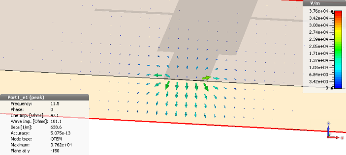
The plot also shows some important properties of the mode such as mode type, propagation constant and line impedance. The port mode at the second port can be visualized in the same manner.
The three-dimensional surface current
distribution on the conductors can be shown by selecting one of the entries
in the 2D/3D Results ![]() Surface Current folder in the navigation tree. The
surface current at a frequency of 15 GHz can thus be visualized by clicking
at the 2D/3D Results
Surface Current folder in the navigation tree. The
surface current at a frequency of 15 GHz can thus be visualized by clicking
at the 2D/3D Results ![]() Surface Current
Surface Current ![]() surface current (f=15) [1] entry:
surface current (f=15) [1] entry:

You can toggle an animation of the currents
on and off by selecting Post Processing:
2D/3D Plot ![]() View Options
View Options ![]() Animate Fields
Animate Fields ![]() . The surface currents
for the other frequencies can be visualized in the same manner.
. The surface currents
for the other frequencies can be visualized in the same manner.
The transient S-Parameter calculation is mainly affected by two sources of numerical inaccuracies:
1. Numerical truncation errors introduced by the finite simulation time interval.
2. Inaccuracies arising from the finite mesh resolution.
In the following section we provide hints on how to minimize these errors and obtain highly accurate results.
o Numerical Truncation Errors Due to Finite Simulation Time Intervals
As a primary result, the transient solver calculates the time varying field distribution that results from excitation with a Gaussian pulse at the input port. Thus the signals at ports are the fundamental results from which the S-Parameters are derived using a Fourier Transform.
Even if the accuracy of the time signals themselves is extremely high, numerical inaccuracies can be introduced by the Fourier Transform that assumes the time signals have completely decayed to zero at the end. If the latter is not the case, a ripple is introduced into the S-Parameters that affects the accuracy of the results. The amplitude of the excitation signal at the end of the simulation time interval is called truncation error. The amplitude of the ripple increases with the truncation error.
Please note that this ripple does not move the location of minima or maxima in the S-Parameter curves. Therefore, if you are only interested in the location of a peak, a larger truncation error is tolerable.
The level of the truncation error can be controlled using the Accuracy setting in the transient solver control dialog box. The default value of 30 dB will usually give sufficiently accurate results for coupler devices. However, to obtain highly accurate results for filter structures it is sometimes necessary to increase the accuracy to 40 dB or 50 dB.
Because increasing the accuracy requirement for the simulation limits the truncation error and increases the simulation time, the accuracy should be specified with care. As a general rule, the following table can be used:
|
Desired Accuracy Level |
Accuracy Setting (Solver control dialog box) |
|
Moderate |
-30dB |
|
High |
-40dB |
|
Very high |
-50dB |
The following rule may also be useful: If you find a large ripple in the S-Parameters, increase the solvers accuracy setting.
o Effect of the Mesh Resolution on the S-Parameters Accuracy
Inaccuracies arising from the finite mesh resolution are usually more difficult to estimate. The only way to ensure the accuracy of the solution is to increase the mesh resolution and recalculate the S-Parameters. If these results no longer change significantly when the mesh density is increased, then convergence has been achieved.
In the example above, you have used the default mesh that has been automatically generated by an expert system. The easiest way to test the accuracy of the results is to use the fully automatic adaptive mesh refinement that can be switched on by checking the Adaptive mesh refinement option in the solver control dialog box:

Please note that the previously selected template has changed the default settings to the energy based adaptive strategy that is more convenient for planar structures. Thus, you only have to activate the Adaptive mesh refinement tool in the Transient Solver Parameters dialog and start the solver again by pressing the Start button.
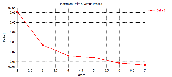
The solver is now running through several
mesh adaptation passes until the desired accuracy limit (2% by default)
is reached. After the mesh adaptation procedure is complete, you
can visualize the maximum difference of the S-Parameters for two subsequent
passes by selecting 1D Results ![]() Adaptive Meshing
Adaptive Meshing ![]() Delta S from the navigation tree:
Delta S from the navigation tree:

In our case, the mesh adaptation was stopped after the second adaptation pass, because the computed change of S-Parameters remained within the specified accuracy limit of 2%.
Visualization of the S-Parameter curves
for different adaptation passes provides deeper insight into the performance
of the mesh adaptation. The following plot is obtained by selecting
1D Results ![]() Adaptive Meshing
Adaptive Meshing ![]() S-Parameters
S-Parameters ![]() S1,1 from the navigation tree and
selecting 1D Plot:
Plot
Type
S1,1 from the navigation tree and
selecting 1D Plot:
Plot
Type ![]() dB
dB ![]() :
:

There was only a small shift in the position of extremal values as the mesh was refined, which demonstrates a good convergence. The convergence process of the other S-Parameters magnitudes and phases can be visualized in the same manner. By inspecting the plots, you can confirm that the important results for the transmission phase are quite stable:

Please note: Refer to the Workflow and Solver Overview manual for information on Template Based Postprocessing for automated extraction and visualization of arbitrary results from various simulation runs.
CST MICROWAVE STUDIO offers a variety of frequency domain solvers that are specialized for different type of problems. They differ not only by their algorithms but also by the grid type they are based on. The general purpose frequency domain solvers are available for hexahedral grids as well as for tetrahedral grids. The availability of a frequency domain solver within the same environment offers a very convenient way to cross-check results produced by the time domain solver with minimal additional effort.
o Making a Copy of Transient Solver Results
Before performing a simulation with a frequency domain solver, you may want to keep the results of the transient solver in order to compare the two simulations. The copy of the current results is obtained as follows: Select, for example, the S-Parameters folder in 1D Results, then press Ctrl+c and Ctrl+v. The copies of the results will be created in the selected folder. The names of the copies will be S1,1_1, S2,1_1 etc. You may rename them to S1,1_TD, S2,1_TD and so on with the Rename command from the context menu. Use Add new tree folder from the context menu to create an extra folder. Please note that at the current time it is not possible to make a copy of 2D or 3D results.
o Optimizing Structure for Tetrahedral Mesh
In the following section, the general
purpose frequency domain solver is applied to the tetrahedral mesh.
This solver is less efficient if there are PEC sheets with very small,
but non zero thicknesses as represented by the stripline in our example.
Because this thickness has a rather small influence on the results compared
to a zero thickness, we rebuild the stripline as a PEC sheet. First,
select the stripline in the navigation tree. Then, turn around the structure
and select the striplines bottom face using the face pick tool Modeling:
Picks ![]() Picks
Picks ![]()
![]() Pick Points,
Edges or Faces:
Pick Points,
Edges or Faces:

Open the Make Shape from Faces dialog
box by selecting Modeling:
Shapes
![]() Faces and Apertures
Faces and Apertures ![]() Shape from Picked Faces...
Shape from Picked Faces...
![]() .
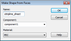
Assign a name to the new shape by entering e.g. stripline_sheet in the
Name field. Press OK to create the new solid.
.
Assign a name to the new shape by entering e.g. stripline_sheet in the
Name field. Press OK to create the new solid.
There may be old results present from the previous transient solver run that will be overwritten when changing the model. In this case, the following warning message appears:
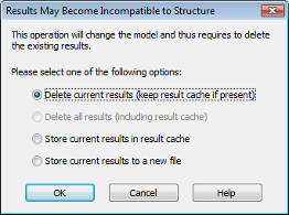
Press OK to acknowledge deletion of the previous results.
Now delete the old solid stripline. Select the solid in the navigation tree and choose Delete from the context menu. It is now time to start the solver.
o Frequency Domain Solver Settings
Open the Frequency Domain Solver Parameters
dialog box by selecting Home:
Simulation ![]() Start Simulation
Start Simulation ![]() Frequency Domain Solver
Frequency Domain Solver ![]() :.
:.

In the Mesh Type combo box you may choose between Hexahedral or Tetrahedral Mesh. Please choose Tetrahedral Mesh. Deactivate the check box of the monitors entry for the adaptation frequency in the Frequency Samples frame. Now you can change the adaptation frequency to 11.5 GHz in the Automatic entry to optimize the mesh at a frequency within the passband of the filter device.
S-Parameters in the frequency domain are obtained by solving the field problem at different frequency samples. These single S-Parameter values are then used by the broadband frequency sweep to obtain the continuous S-Parameter values. The frequency samples are chosen automatically to fit the required accuracy limit throughout the entire frequency band.
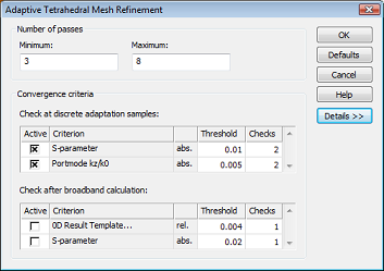
Unlike the time domain solver, the tetrahedral frequency domain solver should always be used with the Adaptive tetrahedral mesh refinement. Otherwise, the initial mesh may lead to a poor accuracy. Therefore, the corresponding check box is activated by default. All other settings should be left unchanged. Everything is now ready; you may press Start to begin the calculation.
During the simulation, the Message Window will show details about the performed simulation. After the maximum number of adaptation passes has been reached, the simulation stops. Nevertheless, the maximum deviation of the S-Parameters is below 1% after the sixth pass.
Congratulations, you have simulated the microstrip phase bridge using the frequency domain solver! Lets review the results.
o 1D Results (S-Parameters)
You can visualize the maximum difference
of the S-Parameters for two subsequent passes by selecting 1D Results
![]() Adaptive Meshing
Adaptive Meshing
![]() f=11.5
f=11.5 ![]() Delta
S from the navigation tree:
Delta
S from the navigation tree:
The S-Parameters
magnitude in dB scale can be plotted by clicking on the 1D Results
![]() S-Parameter folder and selecting
1D Plot:
Plot Type
S-Parameter folder and selecting
1D Plot:
Plot Type
![]() dB
dB ![]() from the tool bar:
from the tool bar:
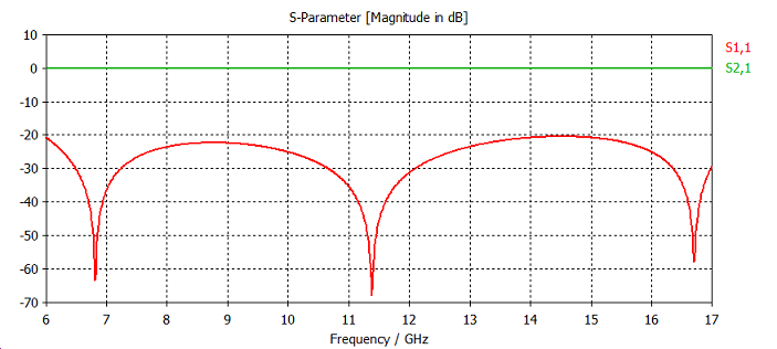
The input reflection S1,1 is quite small (less than 20dB) for almost the entire frequency range.
The most important S-parameter information
for a phase shifter is probably the transmission phase that can be visualized
by clicking on the 1D Results ![]() S-Parameters folder and selecting 1D Plot:
Plot Type
S-Parameters folder and selecting 1D Plot:
Plot Type
![]() Phase
Phase ![]() in the tool bar. If you want to visualize
the phase curve for S2,1 only, you can also select the sub-item 1D
Results
in the tool bar. If you want to visualize
the phase curve for S2,1 only, you can also select the sub-item 1D
Results ![]() S-Parameters
S-Parameters
![]() S2,1:
S2,1:

o 2D and 3D Results (Port Modes and Field Monitors)
Finally, you can observe the 2D and
3D field results. You should first inspect the port modes that can
be easily displayed by opening the 2D/3D Results ![]() Port
Modes
Port
Modes ![]() Port1 folder from the navigation tree. To visualize
the electric field of the fundamental port mode you should click on the
e1 folder. Open the Select
Port Mode dialog box by selecting Select Mode Frequency via the context menu and change
the frequency to 11.5 GHz. Please confirm your setting by pressing
OK. After properly rotating the view
and tuning the settings in the plot properties dialog box, you should
obtain a plot similar to that shown below (please refer to the Workflow and Solver Overview manual for more information on how to change the plots parameters):
Port1 folder from the navigation tree. To visualize
the electric field of the fundamental port mode you should click on the
e1 folder. Open the Select
Port Mode dialog box by selecting Select Mode Frequency via the context menu and change
the frequency to 11.5 GHz. Please confirm your setting by pressing
OK. After properly rotating the view
and tuning the settings in the plot properties dialog box, you should
obtain a plot similar to that shown below (please refer to the Workflow and Solver Overview manual for more information on how to change the plots parameters):
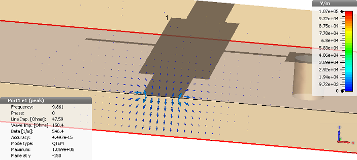
The plot also shows some important properties of the mode such as mode type, propagation constant and line impedance. The port mode at the second port can be visualized in the same manner.
The results of the frequency domain solver using the tetrahedral mesh are mainly affected by the inaccuracies arising from the finite mesh resolution. In the case of a tetrahedral mesh the adaptive mesh refinement is switched on by default. The mesh adaptation is performed by checking the convergence of the S-Parameter values at the highest simulation frequency. The adaptation is oriented towards achieving highly accurate S-Parameter calculations.
If the quality of the results seems unsatisfactory, additional mesh refinement can be performed. For example, three additional mesh adaptation passes can be forced by restarting the frequency domain solver without changing any parameters. Three mesh adaptation passes will be performed according to the Minimum number of passes setting. This setting can be accessed by pressing Properties in the Adaptive Tetrahedral Mesh Refinement frame of the Frequency Domain Solver Parameters dialog:
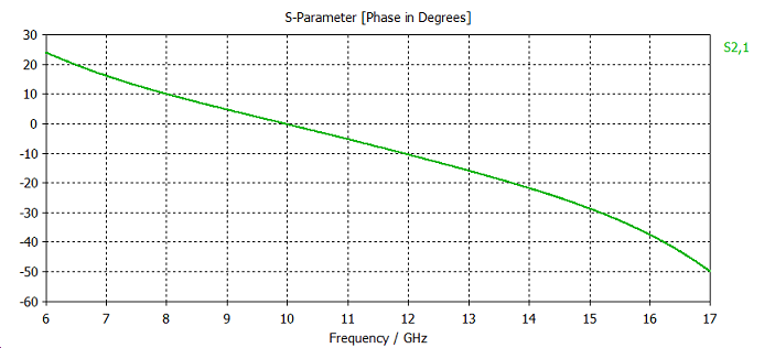
The next plot shows the phase of the S-Parameter S2,1 resulting from the time domain and frequency domain simulations. Plotting the S-Parameter curves in the same graph allows for a better comparison of the results.

As you can see, the results agree very well. Because the results are not converged to the highest possible accuracy level, there is still a slight deviation. This deviation will be reduced when refining the accuracy limit in the adaptive mesh refinement. The difference of the striplines thickness also influences the variations in the S-Parameters.
Congratulations! You have just completed the planar device tutorial that should have provided you with a good working knowledge on how to use the transient solver to calculate S-parameters. The following topics have been covered:
1. General modeling considerations, using templates, etc.
2. Model a planar structure by using the extrude tool, define the substrate and create a via.
3. Define ports.
4. Define frequency range and boundary conditions.
5. Define field monitors for surface current distributions.
6. Start the transient or the frequency domain solver.
7. Visualize port signals and S-Parameters.
8. Visualize port modes and surface currents.
9. Obtain accurate and converged results using the adaptive mesh refinement.
You can obtain more information for each particular step from the online help system that can be activated either by pressing the Help button in each dialog box or by pressing the F1 key at any time to obtain context sensitive information.
In some cases we have referred to the Workflow and Solver Overview manual that is also a good source of information for general topics.
In addition to this tutorial you can find some more S-Parameter calculation examples for planar structures in the examples folder in your installation directory. Each of these examples contains a Readme item in the navigation tree that will give you some more information about the particular device.
Finally, you should refer to the Online documentation for more in-depth information on issues such as the fundamental principles of the simulation method, mesh generation, usage of macros to automate common tasks, etc.
And last but not least: Please also visit one of the training classes held regularly at a location near you. Thank you for using CST MICROWAVE STUDIO!


HFSSЪгЦЕНЬГЬ ADSЪгЦЕНЬГЬ CSTЪгЦЕНЬГЬ Ansoft Designer жаЮФНЬГЬ
|
Copyright © 2006 - 2013 ЮЂВЈEDAЭј, All Rights Reserved вЕЮёСЊЯЕЃКmweda@163.com |
|