![]()
![]()
|
No defect: |
|
|
With defect: |

Introduction and Model Dimensions
In this tutorial, an eddy current sensor is modeled to simulate non-destructive material testing. You will analyze an eddy current sensor driven by a low frequency coil generating eddy currents in an aluminum probe plate. CST EM STUDIO can provide a wide variety of results. This tutorial, however, concentrates solely on the eddy current analysis to detect material defects. The following explanations on modeling and analyzing this device can also be applied to other low frequency problems.
We strongly suggest that you carefully read through the CST EM STUDIO Workflow & Solver Overview manual before starting this tutorial.
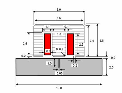
The structure depicted above consists of the sensor, represented by an excitation current coil embedded in iron material. Below this sensor, the probe plate is given as a lossy aluminum material, allowing the flow of eddy currents. Inside this plate a material defect is modeled as a gap that should be detected by the changing voltage at the coil.
This tutorial will guide you through the construction of sensor. For details concerning geometrical constructions please refer also to the online help and the CST EM STUDIO Workflow & Solver Overview manual. Please note that the project file with the complete geometry is delivered with the installation and accessible from the Examples Overview (or the button Run Example at the beginning of this page).
After launching the CST STUDIO SUITE you will enter the
start screen showing you a list of recently opened projects and allowing
you to specify the application which suits your requirements best. The
easiest way to get started is to configure a project template which sets
the basic settings that are meaningful for your typical application. Therefore
click on the Create Project ![]() button in the New Project
section.
button in the New Project
section.
Next you should chose the application area, which is Statics and Low Frequency for the example in this tutorial and then select the workflow by double-clicking on the corresponding entry.

For the eddy current sensor, please select Sensors
![]() Non-Destructive Testing
Non-Destructive Testing ![]() LF
Frequency Domain
LF
Frequency Domain ![]() .
.
At last you are requested to select the units which fit your application best. In this tutorial we will use mm for Dimensions and kHz for the Frequency. For the specific application in this tutorial the other settings can be left unchanged. After clicking the Next button, you can give the project template a name and review a summary of your initial settings.
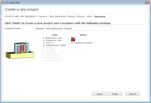
Finally, click the Finish button to save the project template and to create a new project with appropriate settings. CST EM STUDIO will be launched automatically due to the choice of the application area Statics and Low Frequency.
Please note: When you click again on File: New and Recent you will see that the recently defined template appears below the Project Templates section. For further projects in the same application area you can simply click on this template entry to launch CST EM STUDIO with useful basic settings. It is not necessary to define a new template each time. You are now able to start the software with reasonable initial settings quickly with just one click on the corresponding template.
Please note:
All settings made for a project template can be modified later on during
the construction of your model. For example, the units can be modified
in the units dialog box (Home:
Settings ![]() Units
Units ![]() ) and the solver type can be selected in the Home:
Simulation
) and the solver type can be selected in the Home:
Simulation ![]() Start Simulation drop-down list.
Start Simulation drop-down list.
The first construction step for modeling the given device
is to define the probe plate. This can be easily achieved by creating
a brick made of aluminum. To this end, activate the brick creation
mode by clicking Modeling:
Shapes ![]() Brick
Brick
![]() . By pressing the Tab key, you
can enter the coordinates numerically. The plate block has an extension
of 10 mm in each of the transversal directions and is modeled symmetrically
to the origin. Thus, create a brick with
. By pressing the Tab key, you
can enter the coordinates numerically. The plate block has an extension
of 10 mm in each of the transversal directions and is modeled symmetrically
to the origin. Thus, create a brick with
First corner: X = -5, Y = -5 (Xmin, Ymin)
Second corner: X = 5, Y = 5 (Xmax, Ymax)
Height: Zmax = 2 (Zmin = 0)
Finally, the Brick dialog box will appear summarizing all settings. Please assign a meaningful name to the brick by entering e.g. "Plate" in the Name field. Because the brick is the first object you have modeled, you can keep the default settings for the first Component (component1).
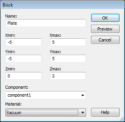
Please note: The use of different components allows you to collect several solids into specific groups, independent of their material behavior.
The Material setting of the brick has to be changed into the desired probe medium. Because no aluminum material has yet been defined, you should select [New Material...] from the Material drop down list to open the New Material Parameters dialog box. There you should define a new Material name (e.g. Aluminum) and set the Type to a Normal material. Furthermore, choose a color for the material by pressing the colored button.
Please note: The defined material Aluminum will be available inside the current project for the further creation of other solids. However, if you want to save this specific material definition for use in other projects, you may check the button Add to material library. You will have access to this material database by clicking on Load from Material Library in the Materials context menu in the Navigation Tree.
Now we must define the material parameters of the Aluminum media. Because only a conductivity has to be set, click on the Conductivity tab to change the dialog page. Please enter an Electric conductivity value of 3.7e7 as shown below:
|
|
|
Confirm your settings by pressing the OK button and again reveal the brick creation dialog box. Here, you can also press the OK button to create the plate brick.
The next step is to model
the gap inside the probe, representing a material defect. We can
do this by creating another brick, as previously shown for the plate. However,
first you should move the drawing plane to the top of the plate. This
can be easily achieved by aligning the working coordinate system (WCS)
with this plane. To this end, select Modeling: WCS
![]() Align WCS
Align WCS ![]() and double-click on the plate's top face (upper z coordinate).
and double-click on the plate's top face (upper z coordinate).
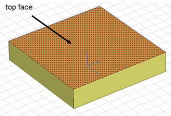
Now the drawing plane will
be aligned with the top of the plate (you may switch off the visualization
of the global coordinate axes by pressing Ctrl+A
or checking Coordinate Axes in
the View: Options![]() View
Options dialog box). Please enter again the brick creation mode
(Modeling:
Shapes
View
Options dialog box). Please enter again the brick creation mode
(Modeling:
Shapes![]() Brick
Brick ![]() ). This time it is suitable to
use the pick point facility to easily adjust the brick's dimensions. Please
select Modeling: Picks
). This time it is suitable to
use the pick point facility to easily adjust the brick's dimensions. Please
select Modeling: Picks![]() Pick
Point
Pick
Point![]() Pick Edge Center
Pick Edge Center ![]() ,
or use the shortcut M
to pick the mid point of the lower U edge by double-clicking
on it. Repeat this procedure to pick the mid point of the upper U edge.
,
or use the shortcut M
to pick the mid point of the lower U edge by double-clicking
on it. Repeat this procedure to pick the mid point of the upper U edge.
|
|
|
Because both picked points have the same V coordinate, the width of the brick is requested. Press the Tab key and enter a value of 0.1 for the Width and leave the dialog by pressing the OK button. Then press the Tab key again to enter the height of the brick. Because the gap should be cut inside the plate, enter a negative value of -1 for the Height and confirm again with OK. Finally, the Brick creation dialog box appears, where you should define a suitable Name for the brick (e.g. Gap) and check the dimensions settings:
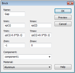
For the moment, we will model the gap as a part of the plate and also designate it as Aluminum material. Therefore, you can just keep the settings of the Component and Material drop-down lists. The brick's material setting will be changed later in order to compare the solver results with and without an air gap.
After confirming the creation of the brick by pressing the OK button, the Shape Intersection dialog appears, where you should select Insert highlighted shape to cut the gap brick into the Plate brick. Note that this operation will preserve the Gap solid whereas Cut away highlighted shape would remove the Gap solid (which is not intended here in order to model the Plate without defect).
|
|
|
Because the sensor is located
slightly above the plate, the Local Coordinate System has to be shifted
slightly in the W direction. Therefore, please select Modeling:
WCS ![]() Transform WCS
Transform WCS ![]() and enter the shift value 0.1 for DW.
and enter the shift value 0.1 for DW.
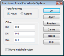
The sensor will now be constructed
from two cylinders. Therefore, please enter the cylinder creation mode
(Modeling:
Shapes ![]() Cylinder
Cylinder ![]() ). Because the center point of the cylinder is given
at the origin of the local coordinate system, you can press the Tab key while holding the Shift
key to initialize the Enter Point
dialog with zeroed values. Accept these settings and again press
the Tab key to define the outer
radius of the cylinder. Please enter a value of 3
for the Radius and confirm this
setting by clicking the OK button.
After pressing the Tab key once
more, you can define the Height
of the cylinder with a value of 3.8.
Finally, skip the inner radius definition by pressing the Esc
key.
). Because the center point of the cylinder is given
at the origin of the local coordinate system, you can press the Tab key while holding the Shift
key to initialize the Enter Point
dialog with zeroed values. Accept these settings and again press
the Tab key to define the outer
radius of the cylinder. Please enter a value of 3
for the Radius and confirm this
setting by clicking the OK button.
After pressing the Tab key once
more, you can define the Height
of the cylinder with a value of 3.8.
Finally, skip the inner radius definition by pressing the Esc
key.
The cylinder creation dialog opens. Again, you may choose a suitable Name for the cylinder (e.g. Sensor). The Sensor should be put into a second component. Therefore select [New Component...] from the Component drop down list. The initial setting for the material is the most recently selected Aluminum media. Therefore, please select [New Material...] from the Material drop-down menu to open the New Material Parameters dialog box. There you can define an iron material for the sensor. First, choose a suitable Material name (e.g. Iron) and set the Type to a Normal material. Additionally, you should enter a value of 100 for the Mue parameter and change the color of the iron material. Then close this dialog box and the Cylinder dialog box by pressing the OK buttons, respectively.
|
|
|
Now we will construct a second
cylinder in order to hollow out the first one. To achieve this, please
again activate the cylinder mode again (Modeling:
Shapes ![]() Cylinder
Cylinder ![]() ) and use the Tab
key to create the second cylinder shape with
) and use the Tab
key to create the second cylinder shape with
center at U=0.0, V=0.0
outer radius of 1.9
height of 2.8
inner radius of 0.8
Because this solid is only used to hollow out the previously defined cylinder, you do not have to consider the Name, Component or Material settings in the Cylinder creation dialog box. Just accept the cylinder's dimension by pressing the OK button. The Shape Intersection dialog informs you that component2:solid1 intersects with component2:Sensor. Please choose Cut away highlighted shape and confirm with OK to create the cavity.
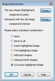
To obtain a better impression
of your model it is useful to switch on the cutting plane by selecting
View:
Sectional View ![]() Cutting Plane
Cutting Plane ![]() or use the shortcut Shift+C.
Your structure should now look similar to the following picture:
or use the shortcut Shift+C.
Your structure should now look similar to the following picture:
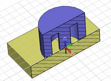
To chamfer the upper edge
of the sensor, choose Modeling: Picks
![]() Picks
Picks ![]() or use the shortcut E. Now double-click
on the upper circle edge of the sensor and select Modeling: Tools
or use the shortcut E. Now double-click
on the upper circle edge of the sensor and select Modeling: Tools
![]() Blend
Blend ![]() Chamfer Edges
Chamfer Edges ![]() .
In the dialog box define a Chamfer width
of 0.2.
.
In the dialog box define a Chamfer width
of 0.2.
|
|
|
|
One more edge of the iron
solid will be modified. This time, however, by blending. Again, activate
the picking tool (Modeling: Picks
![]() Picks
Picks ![]() or shortcut E) and double-click
on the lower circle edge. Then choose Modeling:
Tools
or shortcut E) and double-click
on the lower circle edge. Then choose Modeling:
Tools ![]() Blend
Blend ![]() Blend Edges
Blend Edges ![]() and enter a Radius of 0.2
in the Blend Edges dialog box.
and enter a Radius of 0.2
in the Blend Edges dialog box.
|
|
|
|
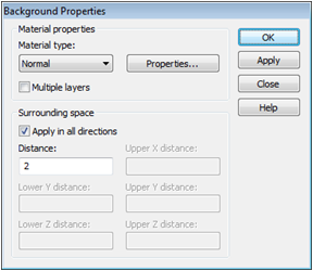
In order to suppress some
influences from the adjacent boundaries, it is advisable to add some extra
space around the complete structure. This can be easily accomplished
by defining proper background material properties in the Background
Properties dialog box (Modeling:
Materials
![]() Background
Background ![]() ). Please select the Material
type Normal, activate
"Apply in all directions"
and enter a value of 2 in the active Distance
field.
). Please select the Material
type Normal, activate
"Apply in all directions"
and enter a value of 2 in the active Distance
field.
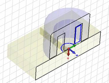
The next step is to add the excitation coil to the model.
This can be easily done with the help of curve definitions. Here we need
one circle (coil path) and one rectangle (coil profile). As for the
cylinder creation, the coordinates can be entered numerically with the
help of the Tab key. Thus, define
a circle (Modeling: Curves
![]() Curves
Curves ![]() Circle
Circle ![]() ) with
) with
Center at X=0.0, Y=0.0 and
Radius 0.9
The created circle curve will be displayed in the Modeler view still showing only half of the structure due to the previously activated cutting plane. Immediately after its creation the curve is selected automatically, so that all solids are plotted transparently to offer a better visualization of the curve.
To define the coil's profile, we must first rotate the
local coordinate system by pressing the Shift
and V key simultaneously or by
selecting Modeling:
WCS ![]() Transform WCS
Transform WCS ![]() and entering
90 in the V
field of the Rotate Transformation type.
and entering
90 in the V
field of the Rotate Transformation type.
Now create a rectangular curve (Modeling: Curves
![]() Curves
Curves ![]() Rectangle
Rectangle ![]() ) with
) with
First point at U = -0.2 and V = 0.9
Second point at U = -2.7 and V = 1.7
Please note that your input settings correspond to the local coordinate system because it is still active. Finally, the structure will now look like this:
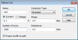
With the help of the two recently created curves, it
is now possible to define a current coil. Please choose Simulation:
Sources and Loads
![]() Coil
Coil ![]() to
enter the coil creation mode. The profile curve has to be selected
first. Each existing curve is highlighted when the mouse cursor is moved
over it. Double-click on the rectangular curve and then on the circle
curve when asked to select the path curve. Now the Define
Coil dialog box appears, where you can define the excitation settings.
to
enter the coil creation mode. The profile curve has to be selected
first. Each existing curve is highlighted when the mouse cursor is moved
over it. Double-click on the rectangular curve and then on the circle
curve when asked to select the path curve. Now the Define
Coil dialog box appears, where you can define the excitation settings.
To apply a total current flow of 100 A in the cross-section of the coil, please enter a Value of 0.1 A and a Number of turns of 1000.
Please note that by default, all source values are interpreted by the low frequency solver as root-mean-square (rms) values. In the LF Frequency Domain Solver dialog box, it is possible to change this setting and to use amplitudes (peak values) for the simulations. However, here we will not make use of this possibility and continue with rms values.
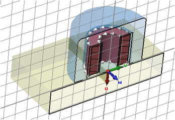
After confirming these settings you can double-check your model with the picture below (in order to obtain a similar view, please select the coil1 item of the Coils folder in the Navigation Tree or just double-click on the coil in the drawing plane):
For the next step, the local coordinate system is no
longer needed, so you may switch it off by clicking on Local
WCS in the Simulation
ribbon. Furthermore, you may also deactivate the cutting plane by selecting
View:
Sectional
View ![]() Cutting Plane (Shift+C)
Cutting Plane (Shift+C)![]() .
.
Electric boundary conditions are required for this model. This setting models a situation when the entire structure (including the background box material) is embedded into a perfectly conducting housing. Of course, keeping in mind that the structure is surrounded by open space, the artificial truncation of the computational domain introduces an additional modeling error. In order to reduce this error, a larger background material box can be defined. Nevertheless, for the tutorial, you should not use a substantially larger box, as doing so would elongate the computation time. However, you should always be aware of the additional truncation error if you aim to model open space problems. For such situations it is advisable to compute the same problem twice using different sizes for the background material box to check if the result of interest will stay unchanged when the box is enlarged.
Please open the Boundary
Conditions dialog box (Simulation: Settings
![]() Boundaries
Boundaries ![]() ) and verify that all Boundaries
are of type electric. Then switch
to the Symmetry Planes tab. Whenever
you have defined a problem in CST EM STUDIO you should check, whether
you can take advantage of symmetries in your model. Remember that a field-solution
will be symmetric with respect to a coordinate plane if
) and verify that all Boundaries
are of type electric. Then switch
to the Symmetry Planes tab. Whenever
you have defined a problem in CST EM STUDIO you should check, whether
you can take advantage of symmetries in your model. Remember that a field-solution
will be symmetric with respect to a coordinate plane if
the structure (geometry and materials),
the defined sources,
and the defined boundary conditions
are all symmetric with respect to this coordinate plane. If this is the case, you can exploit this a priori knowledge to reduce the computational time considerably by defining symmetry planes. Each symmetry plane you define will reduce the problem size by a factor of two.
In the Boundary Conditions dialog box, you can activate two planes and thus reducing the problem size by a factor of four: The model structure is symmetric with respect to the YZ as well as the XZ plane. Moreover, the magnetic field generated by the coil has no normal component at these planes and all boundary conditions are electric. Therefore, the field solution is unaffected if a purely tangential magnetic field is explicitly enforced at these symmetry planes by selecting electric symmetry conditions. For this purpose, select the electric (Et = 0) option from the corresponding drop-down menus. The changes are visualized simultaneously in the drawing plane:
|
|
|
Confirm these settings with the OK button.
A similar example for the application of symmetry planes can be found in the CST EM STUDIO Workflow & Solver Overview manual.
Now the calculation frequency must be defined. For
this purpose, please click on Simulation:
Settings ![]() Frequency
Frequency ![]() to open the Define
Calculation Frequency dialog box. Here you have the possibility
of entering several frequency points for which calculations should be
performed. For this example it is sufficient to determine only one Frequency sample at 12 kHz (corresponding
to the current frequency unit displayed in the status bar). After you
have entered the value press the OK
button.
to open the Define
Calculation Frequency dialog box. Here you have the possibility
of entering several frequency points for which calculations should be
performed. For this example it is sufficient to determine only one Frequency sample at 12 kHz (corresponding
to the current frequency unit displayed in the status bar). After you
have entered the value press the OK
button.
In this tutorial, we will concentrate on the tetrahedral mesh. Because this is the default mesh type, you do not need to change anything.
Enter the Mesh Properties
dialog box by selecting Simulation:
Mesh ![]() Global
Properties
Global
Properties ![]() . To get a reasonable overall mesh resolution of the
problem, set the Min. number of steps
to 15. Do not press OK at this stage.
. To get a reasonable overall mesh resolution of the
problem, set the Min. number of steps
to 15. Do not press OK at this stage.
Along the blended edges of the sensor core, one expects a concentration of the magnetic field. In order to resolve this phenomenon appropriately, it is necessary to resolve the curvature of the blends. Furthermore, the curved coil geometry should be taken into account adequately. To achieve this you may change the default curvature refinement settings by clicking on the Specials button. Select the Surface: General tab and set the Curvature refinement ratio value to 0.02 and the Max. number of steps from curvature ref. to 200.
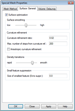
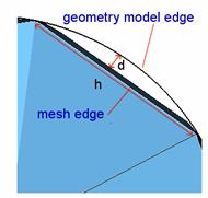
The first value defines an upper bound for the deviation of the mesh geometry from the original curved geometry. More precisely, the mesh size is defined such that the ratio d/h (see following figure) is less than the given value everywhere. Reasonable values for usual applications are in the range from 0.01 to 0.05. The second value is necessary to prevent extremely fine meshes at geometric singularities. It defines how much smaller the mesh size defined by the curvature refinement ratio is allowed to be compared to the original mesh size of the shape. Usual values are in the range of 50 to 500.
After this short introduction to the curvature refinement for tetrahedral meshes, confirm all mesh settings with the OK button.
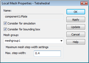
It is important that the tetrahedral mesh resolves the skin depth in the aluminum plate adequately. To ensure this, set local mesh densities: double-click on the Plate solid in the main view and select Local Mesh Properties from the context menu to specify special mesh settings assigned only to the selected solid component1:Plate. Set the Max. step width value to 0.4 and press the OK button.
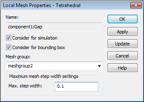
In the same manner, set a local mesh density for the gap: double-click on the Gap solid select Local Mesh Properties from the context menu. Here you may choose an even smaller value. A good choice that leads to an almost isotropic mesh in the gap-solid is the gap-width. Therefore, set the Max. step width value to 0.1 and press the OK button.
Now all mesh adjustments have been performed and you
can start the tetrahedral low frequency solver. Select Simulation:
Solver ![]() Start Simulation
Start Simulation ![]() to open the LF
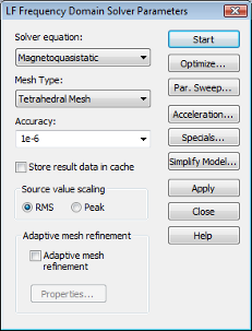
Frequency Domain Solver Parameters dialog box. The Mesh
Type should be set to "Tetrahedral
Mesh". It is not necessary to modify the default
Accuracy value of 1e-6. But
deactivate the Adaptive mesh refinement
for this solver run. Finally, press the Start
button.
to open the LF
Frequency Domain Solver Parameters dialog box. The Mesh
Type should be set to "Tetrahedral
Mesh". It is not necessary to modify the default
Accuracy value of 1e-6. But
deactivate the Adaptive mesh refinement
for this solver run. Finally, press the Start
button.
As the tetrahedral mesh has not yet been generated, the solver will first start the tetrahedral mesh generator. You will see a progress bar displaying the status of the mesh generation.
Please note that the generation of a tetrahedral mesh is usually much more time-consuming than the generation of an hexahedral mesh in CST EM STUDIO because the tetrahedral mesh resolves the geometry explicitly whereas a hexahedral mesh does not. The hexahedral solver resolves the geometry implicitly using the Perfect Boundary Approximation (PBA) technique.
Then, the solver itself will be started. You will receive information on the progress of the solver and the currently performed operation in the Progress or Messages windows. Usually the most time consuming part of the solver run is the solution of the linear system of equations.
Congratulations, you have simulated the eddy current sensor with the tetrahedral solver!
Please note that the results might differ slightly depending on the operating system and the architecture of the machine with which they were computed.
Initially, you may want to inspect the mesh by selecting
Home: Mesh
![]() Mesh View
Mesh View ![]() . Recall that you can switch on or off the
cutting plane with Shift+C.
. Recall that you can switch on or off the
cutting plane with Shift+C.
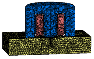
You will recognize that the mesh around the gap and at the curved sensor edges is very fine and that the mesh density in the plate is higher than in the sensor, as expected. The global mesh resolution, however, is moderate, which is sufficient for this example, because the tetrahedral solver uses second-order elements by default leading to a high accuracy. (This setting can be changed in the Specials dialog box of the solver control dialog.)
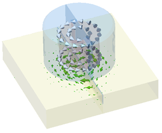
Let's examine the results. Remember that the material of the Gap solid is still Aluminum, i.e. no material defect is modeled with this setting. There are some new entries in the 2D/3D Results folder in the Navigation Tree. Click on the Cond. Current Dens. [12] folder to visualize the three-dimensional arrow plot. Note that you may have to step the phase of the fields to 90° by pressing the right cursor key several times after clicking once in the main view. To get a better view, you can also adjust the arrow object settings in the Objects frame of the 3D Vector Plot dialog box (Select Properties from the Plot ribbon or Plot Properties from the context menu).

To check the voltage value, double-click on the Coil Parameters text info icon in the Navigation Tree:
Coil parameters at frequency [ 12.000 kHz] (load system):
--------------------------------------------------------------
coil1 Current : 1.000000e-001 + i 0.000000e+000 A (rms)
Voltage : 6.444136e+000 + i 7.919333e+001 V (rms)
Impedance: 6.444136e+001 + i 7.919333e+002 Ohm
Power : 6.444136e-001 + i 7.919333e+000 W (rms)
Now let's simulate the material defect. The Gap solid, currently assigned to Aluminum material, should now be changed to Vacuum material: Double-click on the gap solid in the main-view and select Change Material from the context menu. Then select Vacuum from the Material drop down list in the Change Material dialog box. Confirm this setting with OK. You will be asked whether to delete the results. Agree with OK. Now the gap inside the aluminum plate is filled with Vacuum material, which can be seen in the solid description at the lower left corner of the main view when selecting the Gap solid again.
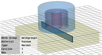
Please restart the tetrahedral solver as before by opening
the solver control dialog box (Simulation:
Solver ![]() Start Simulation
Start Simulation ![]() ) and pressing the Start
button. After the simulation has finished, examine again the computed
eddy currents inside the probe by clicking on the Cond.
Current Dens. [12] entry in the 2D/3D
Results folder of the Navigation
Tree. Remember that you may have to step the phase of the fields
to 90° by pressing the right cursor key several times after clicking once
in the main view.
) and pressing the Start
button. After the simulation has finished, examine again the computed
eddy currents inside the probe by clicking on the Cond.
Current Dens. [12] entry in the 2D/3D
Results folder of the Navigation
Tree. Remember that you may have to step the phase of the fields
to 90° by pressing the right cursor key several times after clicking once
in the main view.
In order to compare the computed coil voltage to the one of the previous solver run without the material defect, click again on the Coil Parameters info text item.
Coil parameters at frequency [ 12.000 kHz] (load system):
--------------------------------------------------------------
coil1 Current : 1.000000e-001 + i 0.000000e+000 A (rms)
Voltage : 5.431043e+000 + i 8.140352e+001 V (rms)
Impedance: 5.431043e+001 + i 8.140352e+002 Ohm
Power : 5.431043e-001 + i 8.140352e+000 W (rms)
There is a difference of approximately 2 V between the absolute voltage values of the two tetrahedral solver runs with and without the gap.
Let us review the meaning of the real and imaginary part of the computed coil voltage. Consider the well-known formula
![]() ,
,
where ![]() and
and ![]() denote the RMS values of the coil-voltage
and the coil-current, respectively,
denote the RMS values of the coil-voltage
and the coil-current, respectively, ![]() denotes the angular frequency,
denotes the angular frequency, ![]() and
and ![]() denote the mean values of the magnetic
energy and the Ohmic losses, respectively.
denote the mean values of the magnetic
energy and the Ohmic losses, respectively.
Hence, one gets the following expression for the coil-voltage:
![]()
Because the coil-current is real-valued in the example, the real part of the coil voltage is proportional to the Ohmic losses in the plate and the imaginary part is proportional to the magnetic energy stored in the system. Please note that for extremely accurate computations of models that include curved coils, the tetrahedral solver is usually more suitable than the hexahedral solver because the current distribution in the coil can be resolved more easily, leading to a faster convergence with respect to the mesh density.
A low frequency field calculation is mainly affected by two sources of numerical inaccuracies:
Numerical errors introduced by the iterative linear equation system solver.
Numerical errors arising from the finite mesh resolution.
In this section we provide some hints how to minimize these errors and achieve highly accurate results.
In most cases (unless the number of the degrees of freedom is very low) CST EM STUDIO uses an iterative linear equation system solver to solve the discretized field problem. The iterative solver will stop a calculation when a given accuracy has been reached. Generally, the accuracy setting of 1e-6 is sufficient for most calculations. However, in some cases the solver will give you a warning that the results are inaccurate
and that you should consider increasing the solver accuracy.
Inaccuracies arising from the finite mesh resolution are usually more difficult to control. One possibility of ensuring the solution accuracy is to compare the results of a hexahedral mesh solver-run with the results of a tetrahedral solver-run.
Another way to ensure the accuracy of the solution is to increase the mesh resolution by a reasonable amount and recalculate the results. When the results no longer significantly change with increasing mesh density, then convergence has been achieved.
The easiest way to test the accuracy of the results is to use fully automatic mesh adaptation that can be switched on by checking the Adaptive mesh refinement option in the solver control dialog box.
In order to keep the single solver runs short in this tutorial we will skip a detailed description of the Adaptive mesh refinement feature here.
Congratulations! You have just completed the tutorial which should have provided you with a good working knowledge on how to use the low frequency solver. The following topics have been covered:
General modeling considerations, using templates, etc.
Model a sensor including probe plate by using the brick and cylinder creation modes.
Define an excitation coil from previously defined curves.
Define symmetry conditions.
Apply changes to the default tetrahedral mesh.
Start the tetrahedral low frequency solver.
Visualize the eddy current fields.
Simulate the model with and without material defect.
You can obtain more information for each particular step from the online help system that can be activated either by pressing the Help button in each dialog box or by pressing the F1 key at any time to obtain context sensitive information.
In some instances we have referred to the CST EM STUDIO Workflow & Solver Overview manual that is also a good source of information for general topics.
In addition to this tutorial you can find more low frequency problems in the examples folder in your installation directory. Each of these examples contains a Readme item in the Navigation Tree that will provide you with more information about the particular device.
And last but not least: Please also visit one of the training classes, held regularly at a location near you. Thank you for using CST EM STUDIO.