
 2D/EDA Files
 Cadence Allegro PCB / APD / SiP
Important notes:
For package layouts (APD/SiP), using the Cadence Plug-in is strongly recommended. Otherwise, some data may be missing (wirebond profiles and BGA dimensions for APD/SiP, die-stacks for APD). Background: Upon import of Cadence APD/SiP layouts, the file "profiles.xml", if present in the design's directory, will be used to include the correct wirebond profiles. If the file is not present, a default profile is used for all wirebonds.
If Cadence and CST software is not installed on the same computer, the Cadence Plug-in can be used to extract the required data from the Cadence layout database into some specified directory. This directory can be transferred to another computer having CST software installed. Then use CST STUDIO SUITE™ to import the contained design.
Only conductors belonging to some net will be imported.
The Cadence Plug-in is a component installed on top of an existing Cadence installation. The plug-in's user interface is then embedded into the corresponding tool environment and allows exporting ASCII files from within the Cadence workflow. The exported ASCII files are required for the import into CST MICROWAVE STUDIO® if no Cadence installation is available.
Installation of the Cadence Plug-in
Exporting Models from Cadence® Allegro PCB / SiP
The Plug-in offers the following options generating a layout export:
Components tab (APD only)
As opposed to Cadence SiP, there is no support for die stacks in Cadence APD. Moreover, the thickness of dies and their bump dimensions (if flip-chip) are not part of the Cadence database. It is therefore important to specify these parameters in the present dialog.
Component
Name of the die (not editable)
Attachment
Displays the die-attachment type (flip-chip or wirebond)
Die Orientation
Denotes the orientation of the die (chip-down if the die pads are on the bottom side)
Diestack
This free number field can be used to group the dies into die stacks. All dies of the same stack carry the same number. Their relative, vertical placement will then be deduced from the database. For a multi-chip module without die stacks, all dies in the list have to carry a different stack number.
Thickness
Specifies the thickness of the die.
Bump Height, Thickness
For flip-chip designs, specifies the height and diameter of the bumps, respectively.
BGA tab
The dimensions of the solder balls to be attached to a ball-grid array are not part of the current Cadence database and can be specified in this tab.
Component
Name of the BGA component
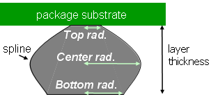
Center rad., Top radius, Bottom rad., Height
Specifies the shape of solder balls/bumps, as can be seen from the following picture.

Package Setup File
This field allows saving and restoring the data entered in the present dialog.
Units
Length unit of all absolute lengths given in this dialog.
This is the easiest way to export the current model.
Define the location of the exported ASCII files on your file system. The directory (it is recommended to create a new one) should be named differently from the original design.
Pressing the "Export" button will start the actual export procedure. The original design file will be copied to the target directory, in order to be later imported in CST MICROWAVE STUDIO®.