|
微波射频仿真设计 |
|
|
微波射频仿真设计 |
|
| 首页 >> Ansoft Designer >> Ansoft Designer在线帮助文档 |
|
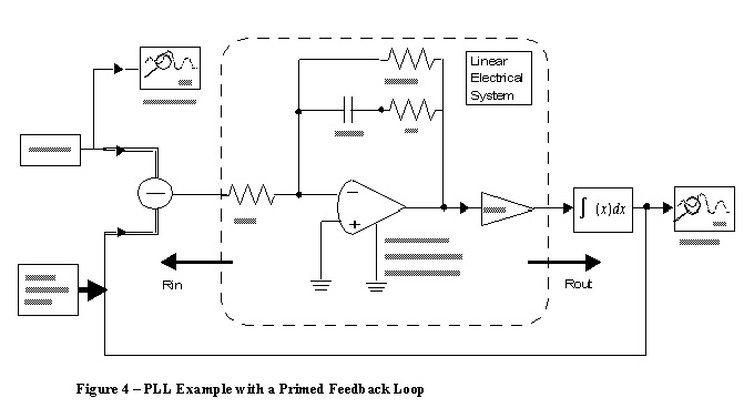
System Simulator > System Partitioning and Scheduling for Simulation PurposesPrior to running the discrete time system simulation, a mixed mode system is partitioned for the purposes of converting a mixed-mode topology to a functional topology where the signal flow is unidirectional. More specifically, the following two classes are modeled functionally or behaviorally (after accounting for all impedance mismatches, noise, and other electrical effects): 1. Linear electrical sub-designs (active and passive). 2. Nonlinear electrical components (amplifiers, mixers and frequency multiplier). Upon finishing the partitioning process (if the system is mixed-mode), the process of scheduling all components inside the system for discrete time simulation begins. Since discrete time signals flow unidirectionally (from input to output), the order in which all components are scheduled is critical during discrete time simulation. The scheduling process always begins with the source components in the system and then iteratively schedules each remaining component (after ensuring that all components leading to the input of that component have already been scheduled). Feedback loops are typically scheduled with the first component in the feed-forward path continuing around the loop until the feedback input is reached. In addition, in order to break the deadlock in the discrete time simulation of feedback loops, the feedback signal in the loop is primed (i.e., stuffed with one discrete time sample at time 0 sec having a zero value). The user instead can force the priming to occur anywhere inside the feedback loop by placing an RDELAY or CDELAY component at the desired priming point. If the simulator does not detect the presence of any RDELAY or CDELAY components in the feedback loop, it will automatically perform the minimum number of primings needed to resolve the deadlock. An example of a simple feedback loop is the phase locked loop example (project pll2) shown below in Figure 4.
To break the deadlock, the feedback signal leading to the input of the CSUB (complex subtractor) component is initially primed with a zero sample.
HFSS视频教程 ADS视频教程 CST视频教程 Ansoft Designer 中文教程 |
|
Copyright © 2006 - 2013 微波EDA网, All Rights Reserved 业务联系:mweda@163.com |
|